

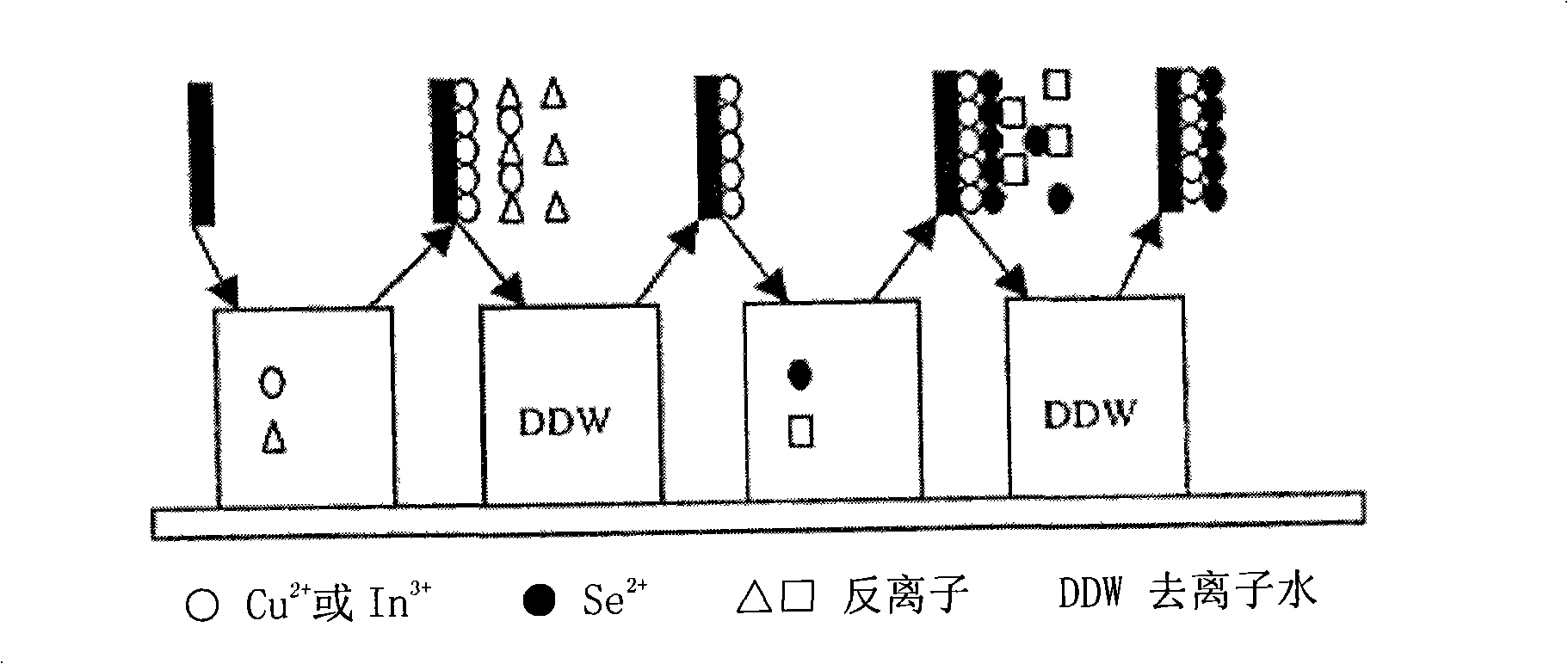
Method for preparing copper indium selenium compound thin film by continuous ion sheath adsorption reaction method
An adsorption reaction, continuous ion technology, applied in chemical instruments and methods, sustainable manufacturing/processing, climate sustainability, etc., can solve problems such as inability to achieve coating, research and application limitations, and achieve good morphology and expanded use. range effect
- Summary
- Abstract
- Description
- Claims
- Application Information
AI Technical Summary
Problems solved by technology
Method used
Image

Examples
Embodiment Construction
[0024] The embodiment of the present invention uses chemically pure raw materials, the precursor solution is 100ml, the cycle is 100 times, and the heat treatment is at 400°C for 1h under the protection of Ar atmosphere. The substrate is ZnO, indium tin oxide (ITO glass), SnO 2 、TiO 2 , ordinary glass or silicon wafer. See Table 1 for details.
[0025] Table 1
[0026]
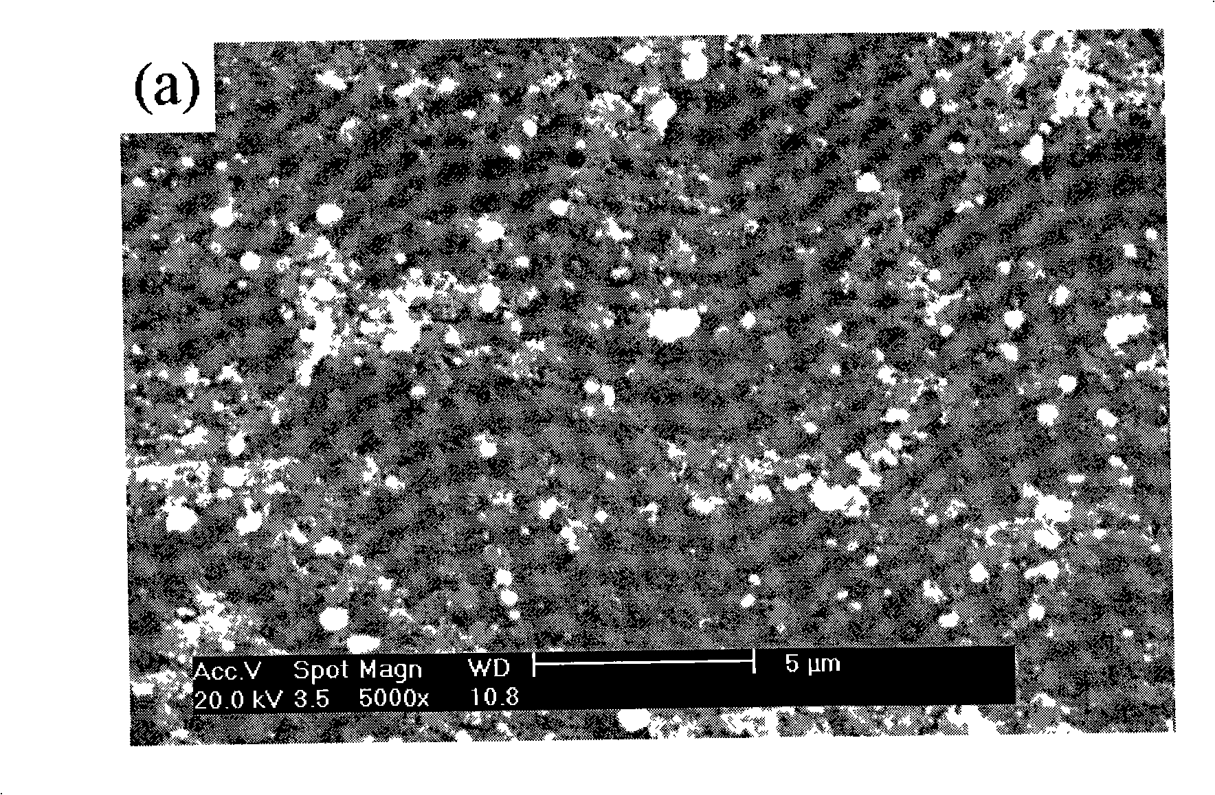
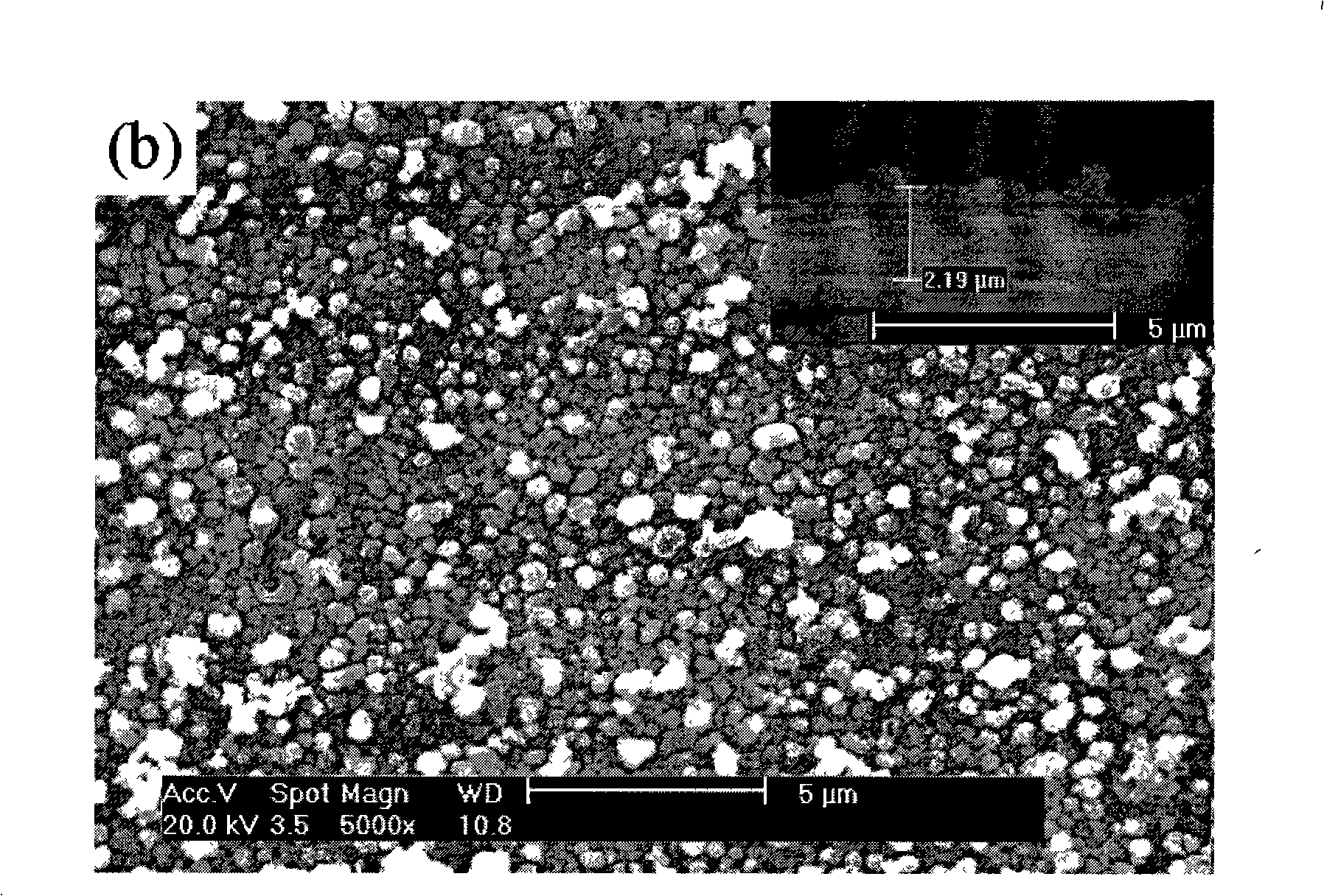
[0027] The materials obtained in the above examples all appear CuInSe 2Phase, by x-ray diffraction (D / MAX-2500x-ray diffractometer) test shows, 1#, 3#, 4# and 6# gained films do not have other miscellaneous phases, by x-ray photoelectron spectrum (Esca MultiplexPhilips-1600x-ray photoelectron spectrum Instrument) test shows, 1#, 4# and 6# film component molar ratio is close to Cu:In:Se=1:1:2. Draw by ultraviolet-visible spectrum analysis (Beckman Du-8B ultraviolet-visible absorption spectrometer), except that the light absorption coefficient of 2# sample is all greater than 10 5 , and the corresponding...
PUM
 Abstract
Description
Claims
Application Information