
Method for producing boron carbide film with electron beam evaporation technique

A technology of electron beam evaporation and boron carbide, which is applied in the direction of vacuum evaporation plating, ion implantation plating, metal material coating technology, etc., can solve the difficulty of meeting the performance requirements of bulletproof materials and wear-resistant materials, and the difficulty of preparing boron carbide films. Difficult to achieve crystal structure and other problems, to achieve the effect of easy control, convenient operation and wide application

Inactive Publication Date: 2008-12-03
SICHUAN UNIV
View PDF0 Cites 10 Cited by
  • Summary
  • Abstract
  • Description
  • Claims
  • Application Information

AI Technical Summary

Problems solved by technology

Although radio frequency magnetron sputtering, microwave method and ion sputtering method in PVD method can be deposited at a lower substrate temperature, which broadens the selection range of substrate materials, most of the deposited boron carbide films are amorphous. , it is difficult to realize the crystalline structure, the hardness is not high enough, and it is difficult to meet the performance requirements of bulletproof materials and wear-resistant materials. In addition, the preparation process of these methods is relatively complicated, and it is very difficult to prepare boron carbide films with different structures; the vacuum in the PVD method There is no report on the preparation of boron carbide thin film by evaporation coating method

Method used


Image

  • Method for producing boron carbide film with electron beam evaporation technique
  • Method for producing boron carbide film with electron beam evaporation technique
  • Method for producing boron carbide film with electron beam evaporation technique

Examples


Embodiment 1

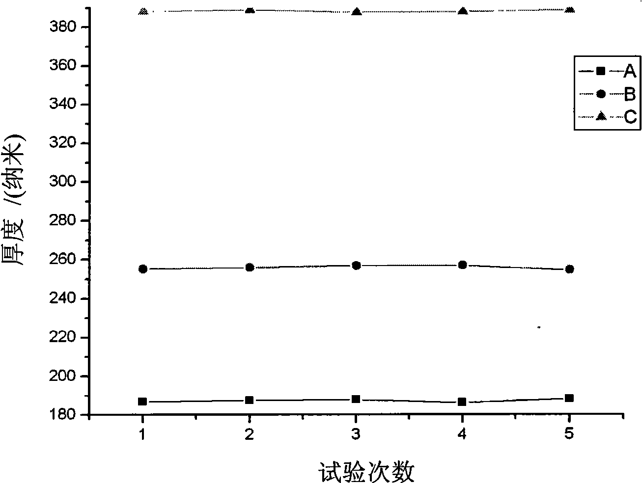
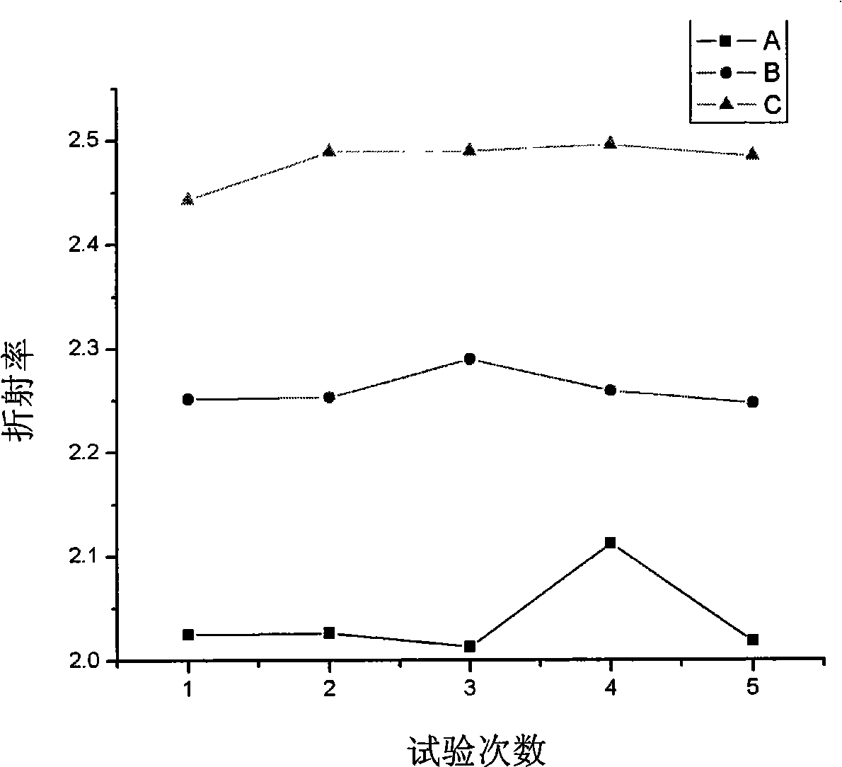
[0025] Under different electron beam currents (electron gun energy), a thin film of boron carbide is deposited on the silicon substrate.

[0026] (1) Preparation of membrane material

[0027] The raw materials are boron powder with a purity of 99.9% and carbon powder with a purity of 99.99%. The molar ratio of carbon powder to boron powder is 1:4; the carbon powder and boron powder are ball milled for 1 hour, mixed evenly, and then placed in a vacuum sintering furnace Sintering, the vacuum degree is 0.01 Pa, the temperature is raised from room temperature to 1900°C at a heating rate of 30°C / min, the holding time is 1 hour, and the temperature is lowered to room temperature at a cooling rate of 20°C / min after holding to obtain boron carbide powder. The boron carbide powder is pressed into a disc (the disc diameter is 20mm, the thickness is 40mm), and the disc is densified at 200MPa isostatic pressing (5 minutes) and then sintered in a vacuum sintering furnace with a vacuum of 0.1Pa...

Embodiment 2

[0033] Change the substrate temperature, and deposit a boron carbide film on the silicon substrate.

[0034] (1) Preparation of membrane material

[0035] The raw materials, process steps and process parameters are the same as in Example 1.

[0036] (2) Coating

[0037] Put the boron carbide film material prepared in step (1) into the crucible of the electron beam evaporation equipment, and put the cleaned and dried silicon substrate F on the heating furnace of the electron beam evaporation equipment, so that the substrate is located 30cm directly above the crucible Place; close the bell jar and vacuum to 1×10 -2 Pa, turn on the bake switch, bake in the vacuum chamber for 10 minutes, heat the silicon substrate, and control the substrate temperature at 25°C (room temperature); continue to vacuum, when the vacuum degree reaches 1×10 -3 At Pa, turn on the power switch and filament switch on the electric control cabinet in order, adjust the filament current at 0.5A, and preheat for 10...

Embodiment 3

[0041] Change the deposition time and deposit a boron carbide film on the silicon substrate.

[0042] (1) Preparation of membrane material

[0043] The raw materials, process steps and process parameters are the same as in Example 1.

[0044] (2) Coating

[0045] Put the boron carbide film material prepared in step (1) into the crucible of the electron beam evaporation equipment, and put the cleaned and dried silicon substrate L on the heating furnace of the electron beam evaporation equipment, so that the substrate is located 30cm above the crucible Place; close the bell jar and vacuum to 1×10 -2 Pa, turn on the bake switch, bake the vacuum chamber for 10 minutes, heat the silicon substrate, and control the substrate temperature at 250°C; continue to vacuum, when the vacuum degree reaches 1×10 -3 At Pa, turn on the power switch and filament switch on the electric control cabinet in order, adjust the beam current to 0.5A, and preheat for 10 minutes; turn on the deflection and focu...


PUM

PropertyMeasurementUnit
densityaaaaaaaaaa
densityaaaaaaaaaa
surface roughnessaaaaaaaaaa

Abstract

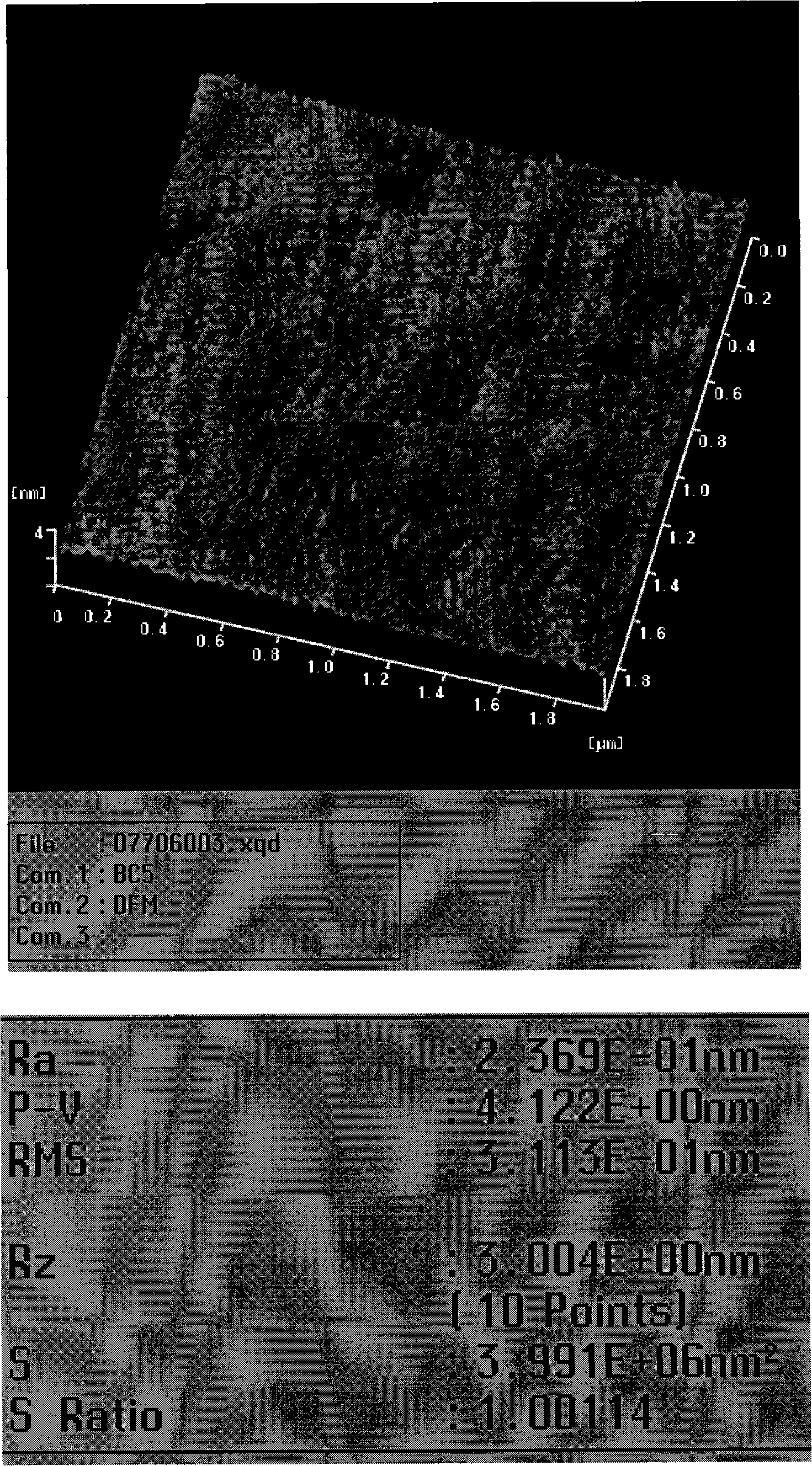
The invention relates to a method for preparing a boron carbide film by using the electron beam evaporation technology. Boron carbide film material is put in a copple of an electron beam evaporation device, and a substrate which is washed and dried is put on a heating electric furnace of the electron beam evaporation device to lead the substrate to be over the copple, the distance of which is 20 to 30cm from the copple; the filming is executed under the vacuum condition, the filming vacuum degree is more than or equal to 6.0*10<minus 3>Pa, and the temperature of the substrate is controlled between room temperature and 450 DEG C; an electron beam is adjusted to lead the focusing spot on the film material to be smallest; the flux distribution is controlled between 100 to 180mA, and the deposition time is 5 to 120 minutes. The method not only can prepare an amorphous boron carbide film, but also can prepare the boron carbide film with a polycrystalline structure, and also can prepare various boron carbide films with different proportions of B and C components, the surfaces of the prepared boron carbide films are smooth, the films are compact, and the uniformity is good.

Description

Technical field [0001] The invention belongs to the field of preparing boron carbide thin films, and particularly relates to a method for preparing boron carbide thin films by electron beam evaporation technology. Background technique [0002] Boron carbide film has high hardness, high modulus, good abrasion resistance, oxidation resistance, strong acid and alkali resistance, and good neutron absorption performance, and has high transmittance to infrared (IR). Laser energy conversion efficiency is high, and it has been widely used at home and abroad as bulletproof materials, anti-radiation materials, wear-resistant and self-lubricating materials, special acid and alkali resistant materials, cutting and grinding tools, and atomic reactor control and shielding materials. The preparation methods of boron carbide films mainly include chemical vapor deposition (CVD) and physical vapor deposition (PVD). The boron carbide films prepared by CVD are crystalline and have high hardness, but...

Claims


Application Information

Patent Timeline
Patent Type & Authority Applications(China)
IPC IPC(8): C23C14/24C23C14/06
Inventor 廖志君刘振良杨水长卢铁城伍登学范强刘成士赵利利
Owner SICHUAN UNIV
Learn More