Wool-making agent for monocrystalline silicon solar cell surface treatment and manufacturing method thereof
A solar cell and surface treatment technology, which is applied in the fields of final product manufacturing, sustainable manufacturing/processing, semiconductor/solid-state device manufacturing, etc., can solve problems such as unstable texturing effect, easy to pollute the production environment, and difficulty in controlling the yield. Achieve the effect of improving photoelectric conversion efficiency, shortening process time and improving work efficiency
- Summary
- Abstract
- Description
- Claims
- Application Information
AI Technical Summary
Problems solved by technology
Method used
Image
Examples
Embodiment 1
[0022] First add 94.0kg of deionized water into the dispersing pot, add 4kg of potassium hydroxide, 50ppm octylphenol polyoxyethylene ether, and 2kg of sodium silicate under stirring, stir for 20 minutes, make it completely dissolve, filter, and discharge to obtain the prepared fleece agent.
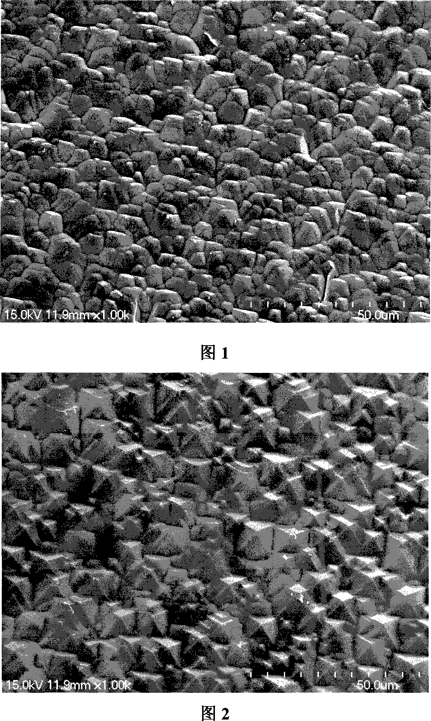
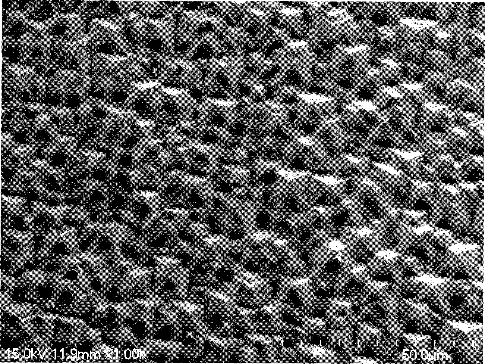
[0023] Take a P-type (100) crystal plane Czochralski monocrystalline silicon wafer, firstly carry out surface cleaning, then put the silicon wafer into the above-mentioned prepared texturizing agent, etch at 80°C for 20 minutes, and the etched silicon wafer is removed Rinse with ionized water to complete the surface treatment. Such as figure 1 It can be seen that a pyramid structure is formed on the surface of the silicon wafer with uniform size and high coverage.
Embodiment 2
[0025] First add 98.0kg deionized water into the dispersing pot, add 1.5kg sodium hydroxide, 1ppm nonylphenol polyoxyethylene ether, and 0.5kg sodium silicate under stirring, stir for 10 minutes to completely dissolve, filter, and discharge. Get velvet.
[0026] Take a P-type (100) crystal plane Czochralski monocrystalline silicon wafer, firstly carry out surface cleaning, then put the silicon wafer into the above-mentioned prepared texturizing agent, etch at 50°C for 60 minutes, and the etched silicon wafer is removed Rinse with ion water to complete the surface treatment.
Embodiment 3
[0028] First add 85.0kg of deionized water into the dispersing pot, add 10kg of potassium hydroxide, 200ppm nonylphenol polyoxyethylene ether, and 5kg of sodium silicate under stirring, stir for 30 minutes, make it completely dissolve, filter, and discharge to obtain the prepared fleece agent.
[0029] Take a P-type (100) crystal plane Czochralski monocrystalline silicon wafer, firstly carry out surface cleaning, then put the silicon wafer into the above-mentioned prepared texturizing agent, etch at 100°C for 2 minutes, and the etched silicon wafer is removed Rinse with ion water to complete the surface treatment.
PUM
 Abstract
Description
Claims
Application Information


