Slot type MOSFET and manufacturing method thereof

An oxide semiconductor and field effect transistor technology, which is applied in the field of trench metal oxide semiconductor field effect transistors and their manufacturing, can solve the problems of difficult processing and high cost, and achieves improved production efficiency, improved welding speed, and reduced usage quantity. Effect

Active Publication Date: 2009-03-11
SHENZHEN JINGDAO ELECTRONICS
View PDF0 Cites 9 Cited by
  • Summary
  • Abstract
  • Description
  • Claims
  • Application Information

AI Technical Summary

Problems solved by technology

[0005] In view of this, it is necessary to provide a method for manufacturing trench metal-oxide-semiconductor field-

Method used


Image

  • Slot type MOSFET and manufacturing method thereof
  • Slot type MOSFET and manufacturing method thereof

Examples


Example Embodiment

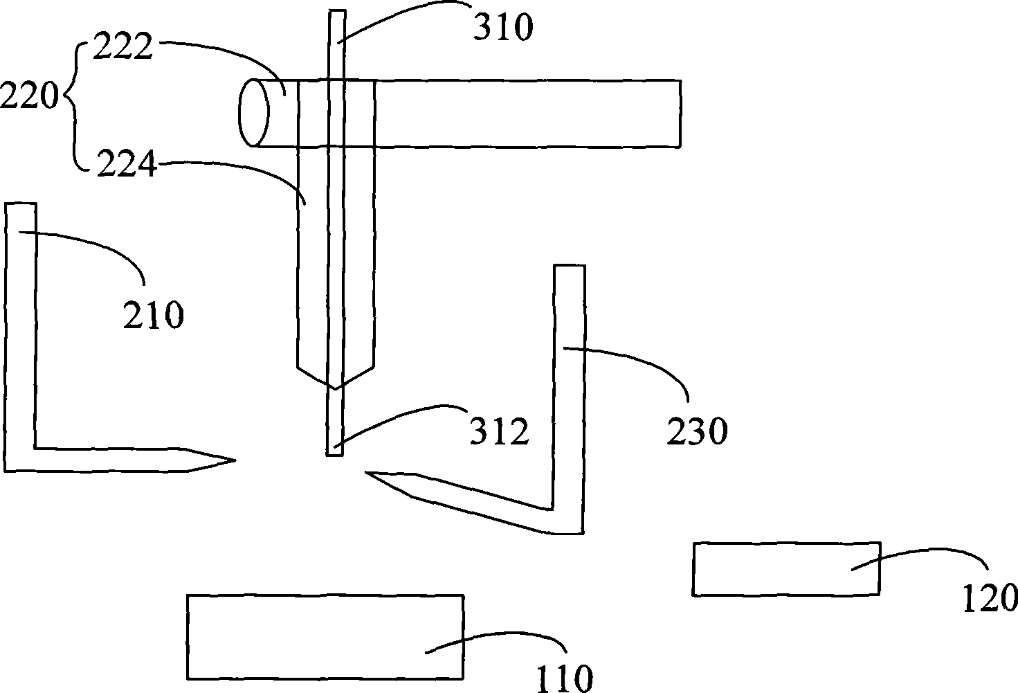
[0022] A detailed description will be given below with reference to specific embodiments. In the following embodiments, copper wires are used to replace traditional gold wires or aluminum wires, so as to achieve the purpose of reducing cost and processing difficulty.

[0023] One of the significant advantages of copper is that its electrical conductivity is better than that of gold and much higher than that of aluminum. Therefore, the amount of copper wire can be reduced to reduce the cost of raw materials. Since Trench MOSFET is a power tube, the current is very large in practical applications, and due to technical limitations, the maximum wire diameter used for ball bonding does not exceed 3 mil (1 mil is one thousandth of an inch, and gold wire can usually only be used 2 mil), so this The method actually requires as many as 12 or more 2mil gold wires to be soldered, so the cost is extremely high and the efficiency is very low. Based on the consideration of reducing cost and...


PUM


Abstract

The invention relates to a method for preparing a groove type metal oxide semiconductor field effect transistor, which comprises the following steps: one end of a copper wire near a chip is melted into a welding ball which is welded on the chip by exerting ultrasonic sound and pressure, and the other end of the copper wire is welded on a frame of the groove type metal oxide semiconductor field effect transistor by using the ultrasonic sound and the pressure. In the groove type metal oxide semiconductor field effect transistor and the preparing method thereof, the copper wire is used for welding, because the electric conductivity of the copper wire is superior to that of gold and aluminium, the copper wire is used for replacing a gold wire, and the cost can be greatly reduced. The preparing method breaks through the forbidden zone that the traditional copper wire ball welding can not be used for a Trench MOSFET technology, and moreover, the invention also provides the groove type metal oxide semiconductor field effect transistor.

Description

【Technical field】 [0001] The invention relates to the technical field of electronic components, in particular to a trench metal oxide semiconductor field effect transistor and a manufacturing method thereof. 【Background technique】 [0002] Field Effect Transistor (Field Effect Transistor) is a semiconductor device that uses the electric field effect to control the magnitude of the current. Field effect tubes are small in size, light in weight, low in power consumption, long in life, and have the advantages of high input impedance, low noise, good thermal stability, strong radiation resistance and simple manufacturing process, so they have a wide range of applications. [0003] In the processing and manufacturing process of field effect transistors, bonding is an important process, which is to conduct conductive connection between the pads (PAD) on the chip and the lead frame (LEADFRAME). Traditionally, gold wire ball welding or room temperature ultrasonic welding are usuall...

Claims


Application Information

Patent Timeline
IPC IPC(8): H01L21/607H01L23/488
CPCH01L2924/3011H01L2224/45147H01L2224/45124H01L2224/45144H01L2924/00011H01L2924/00014H01L2924/01015H01L2924/13091
Inventor 赖辉朋何建欢高燕辉
Owner SHENZHEN JINGDAO ELECTRONICS
Why Eureka
Try Eureka