Check patentability & draft patents in minutes with Patsnap Eureka AI!

Passivation film of composite semiconductor silicon device and passivation generating process

A technology for generating process and silicon devices, which is applied in the fields of semiconductor devices, semiconductor/solid-state device manufacturing, semiconductor/solid-state device components, etc., and can solve the problems of poor particle penetration resistance, affecting reliability, and high defect density at the interface. Achieve excellent optoelectronic properties, reduce soft breakdown and high density

Inactive Publication Date: 2009-03-11
深圳深爱半导体股份有限公司
View PDF0 Cites 4 Cited by
  • Summary
  • Abstract
  • Description
  • Claims
  • Application Information

AI Technical Summary

Problems solved by technology

But on the other hand, SiO 2 Poor particle penetration resistance, radiation sensitivity, and pure SiO 2 Membrane is extremely difficult to generate which limits the application of this membrane
Most of the other films need to be formed by deposition, spin coating, etc., the film formation is loose and the stress is quite different from that of silicon, which makes it poor in blocking impurity diffusion, and the defect density at the interface is high after annealing, so that the section There are many charged particles and trap charges at the interface, which lead to soft breakdown and large leakage in the device characteristic curve after passivation, and affect the reliability in later use.

Method used


Image

  • Passivation film of composite semiconductor silicon device and passivation generating process
  • Passivation film of composite semiconductor silicon device and passivation generating process
  • Passivation film of composite semiconductor silicon device and passivation generating process

Examples


Embodiment 1

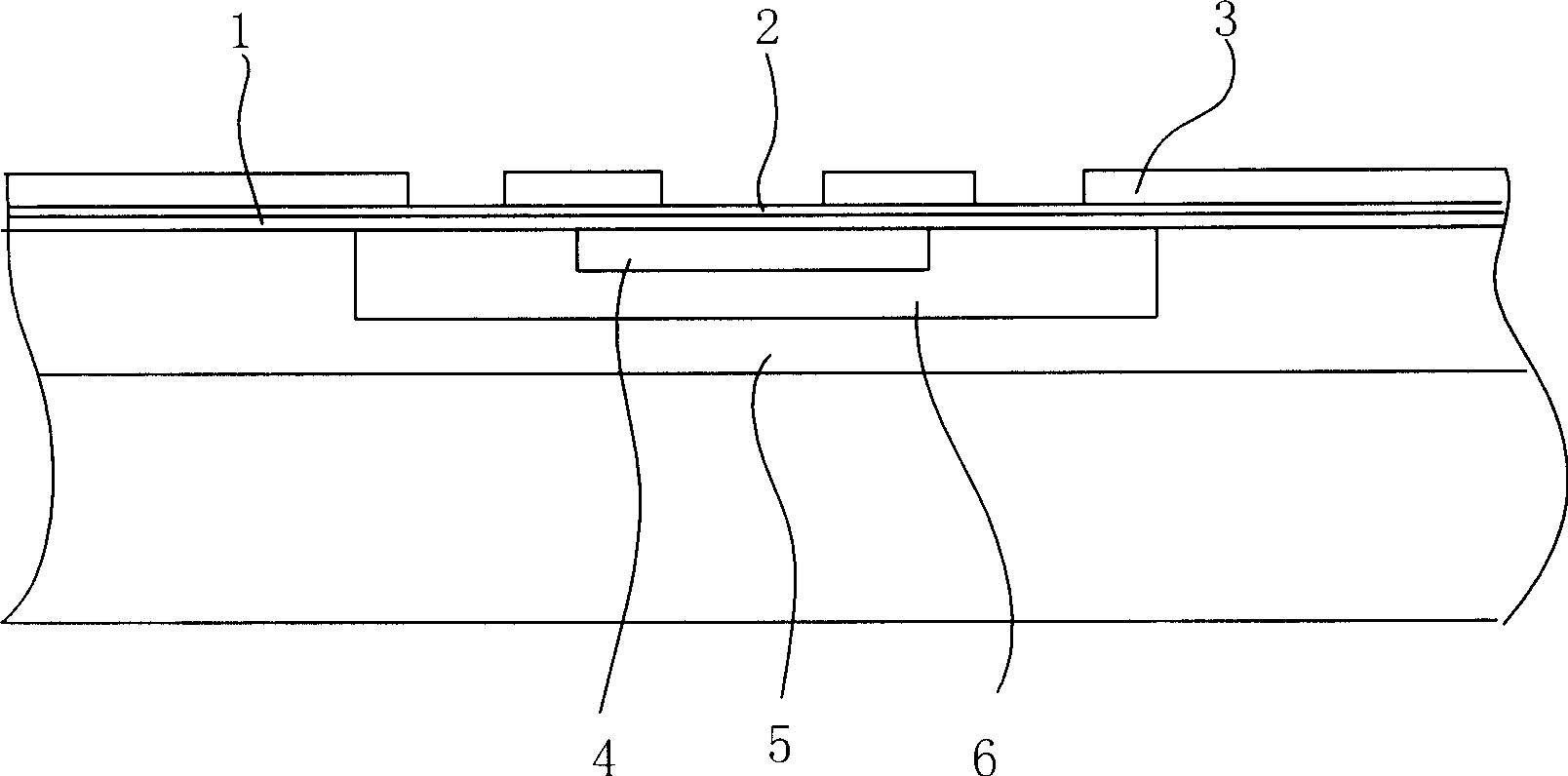
[0024] An oxygen-rich SiOxNy (silicon oxynitride) film layer is formed on the silicon substrate with nodes, and the film thickness is 2000 angstroms. The oxygen-enriched SiOxNy film is formed by low-pressure chemical vapor deposition. It is formed in a low-pressure environment of 280 mTorr and a temperature of 620 degrees Celsius, and a certain ratio of N 2 O and SiH 4 generate. Its atomic content ratio is: Si:O:N=75:20:5. The oxygen-rich SiOxNy film has a stress similar to that of the silicon substrate, which greatly reduces the number of defects at the interface; and its high density makes it have a strong ability to block particle penetration, which limits the charge at the interface. increase in particles. The above two points jointly ensure the stability of the state of the device interface.

[0025] After the lower oxygen-enriched SiOxNy film is formed, a certain amount of N 2 O, SiH 4 and NH3 to re-grow a nitrogen-enriched SiOxNy film layer whose stress is close ...

Embodiment 2

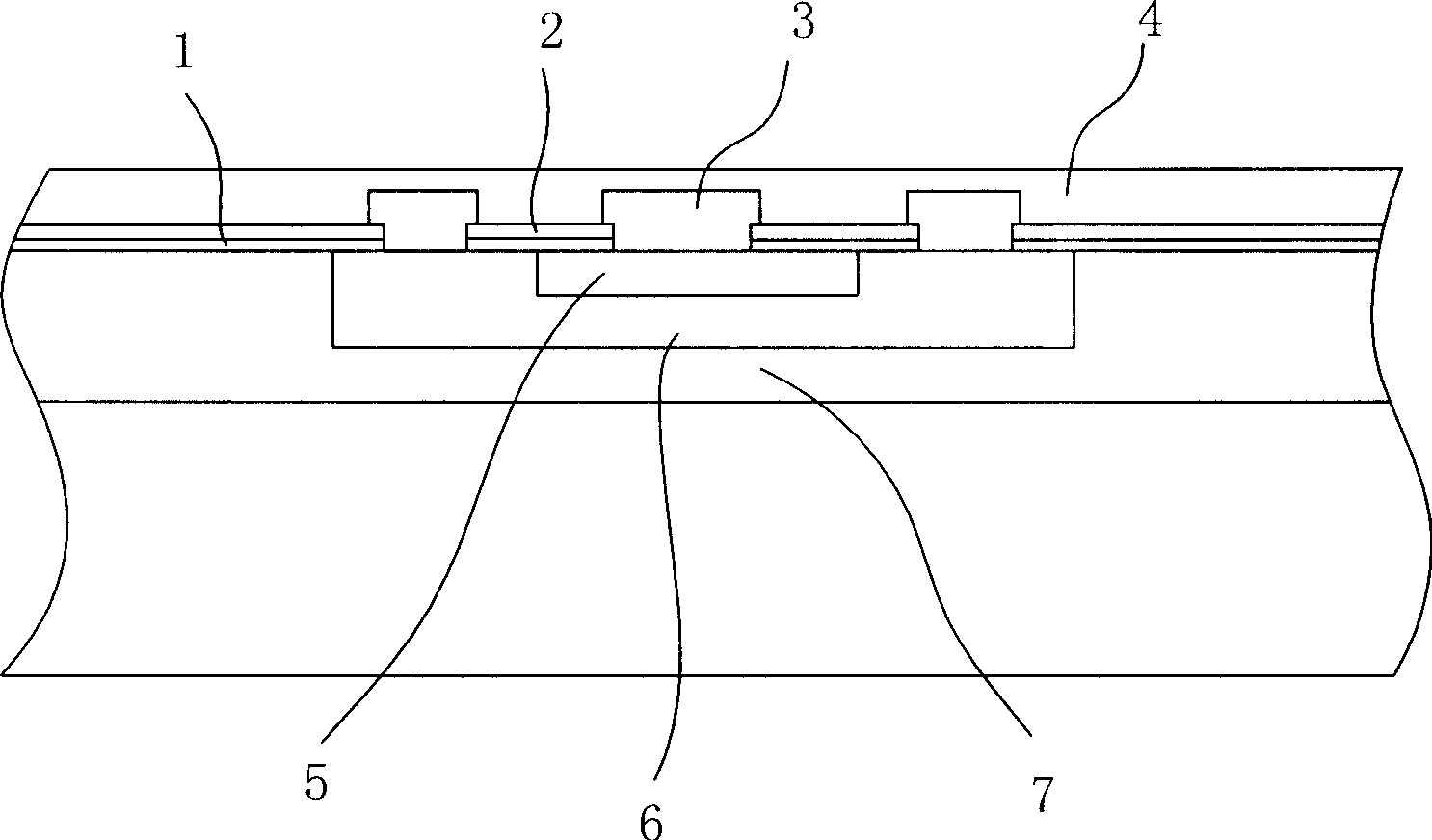
[0032]An oxygen-rich SiOxNy (silicon oxynitride) film layer is formed on the silicon substrate with nodes, and the film thickness is 3500 angstroms. The film is formed by low-pressure chemical vapor deposition. It is formed by feeding a certain ratio of N2O and SiH4 in a low-pressure environment of 310 millitorr and a temperature of 645 degrees Celsius. Its atomic content percentage is: Si:O:N=65:30:5. The film has a stress similar to that of the silicon substrate, which greatly reduces the number of defects at the interface; and its high density makes it have a strong ability to block particle penetration, which limits the increase of charged particles at the interface. The above two points jointly ensure the stability of the state of the device interface.

[0033] After the upper film of the composite film is formed, the process conditions are changed in the same deposition furnace, that is, the temperature is raised to 770 degrees Celsius, and a certain amount of N2O, SiH...

Embodiment 3

[0037] An oxygen-rich SiOxNy (silicon oxynitride) film layer is formed on the silicon substrate with nodes, and the film thickness is 5000 angstroms. The film is formed by low-pressure chemical vapor deposition. It is formed by feeding a certain ratio of N2O and SiH4 in a low-pressure environment of 340 millitorr and a temperature of 670 degrees Celsius. Its atomic content percentage is: Si:O:N=55:40:5. The film has a stress similar to that of the silicon substrate, which greatly reduces the number of defects at the interface; and its high density makes it have a strong ability to block particle penetration, which limits the increase of charged particles at the interface. The above two points jointly ensure the stability of the state of the device interface.

[0038] After the upper film of the composite film is formed, the process conditions are changed in the same deposition furnace, that is, the temperature is raised to 800 degrees Celsius, and a certain amount of N2O, Si...


PUM

PropertyMeasurementUnit
Thicknessaaaaaaaaaa
Thicknessaaaaaaaaaa
Thicknessaaaaaaaaaa

Abstract

The invention relates to a passivation film of a compound type semiconductor silicon device and a passivation generating technology, which belong to the technical field of semiconductor production. The passivation film of the compound type semiconductor silicon device comprises an upper layer film and a lower layer film which are reserved on the section of a silicon base by a photoetching technology, wherein the upper layer film is a nitrogen enriched SiOxNy film, and the lower layer film is an oxygen enriched SiOxNy film. The generating technology comprises the steps: a compact lower oxygen enriched SiOxNy film layer is generated on the silicon base with the section by using a low-pressure chemical gas deposition method, and the stress of the compact lower oxygen enriched SiOxNy film layer is similar to that of silicon; N2O, SiH4 and NH3 are introduced in the same deposition furnace at high temperature of about 740 to 800 DEG C under the environment of 280 to 340 milliliters to grow a nitrogen enriched SiOxNy film layer, the stress of which is close to the stress of the lower oxygen enriched SiOxNy film layer; and after the compound film is finally formed, an SiOxNy compound film on the section of the silicon base is reserved by the photoetching technology. The invention has the advantages of thermal shock resistance, corrosion resistance, creep resistance, oxidation resistance, low expansion, good photoelectric property, and the like.

Description

Technical field: [0001] The invention relates to a compound semiconductor silicon device passivation film and a passivation production process, belonging to the technical field of semiconductor production, in particular to a passivation film on a semiconductor silicon device node and a film production process. Background technique: [0002] In semiconductor silicon devices, regions with different doping elements and different doping concentrations are formed through doping and diffusion. Two such different regions form a PN node or a heterogeneous node. Semiconductor silicon devices are composed of different combinations of PN junctions or heterojunctions. Due to the high sensitivity of semiconductors to impurities, a small amount of external impurity contamination or defects at the interface will cause instability or failure of the electrical parameters of the device. Therefore, for a semiconductor device, passivation and isolation technology directly determine its reliab...

Claims


Application Information

Patent Timeline
IPC IPC(8): H01L23/00H01L29/732H01L21/314H01L21/331
Inventor 张中华
Owner 深圳深爱半导体股份有限公司
Features
  • R&D
  • Intellectual Property
  • Life Sciences
  • Materials
  • Tech Scout
  • Unparalleled Data Quality
  • Higher Quality Content
  • 60% Fewer Hallucinations
Learn More