Method for epitaxial growth of nitride films

A technology of epitaxial growth and nitride, which is applied in the field of semiconductors, can solve the problems of affecting material crystal quality, material crystal quality deterioration, low mobility, etc., and achieve the effect of improving crystal quality and uniformity, reducing growth time, and improving growth efficiency

Inactive Publication Date: 2009-06-03
INST OF SEMICONDUCTORS - CHINESE ACAD OF SCI
View PDF1 Cites 25 Cited by
  • Summary
  • Abstract
  • Description
  • Claims
  • Application Information

AI Technical Summary

Problems solved by technology

However, for nitride film materials containing Al and In, due to the difference in the surface migration rate of adatoms Al and In on the growth substrate, the combination of component elements in the nitride film containing Al and In is affected, and the crystal of the material qua...

Method used


Image

  • Method for epitaxial growth of nitride films
  • Method for epitaxial growth of nitride films
  • Method for epitaxial growth of nitride films

Examples


Embodiment 1

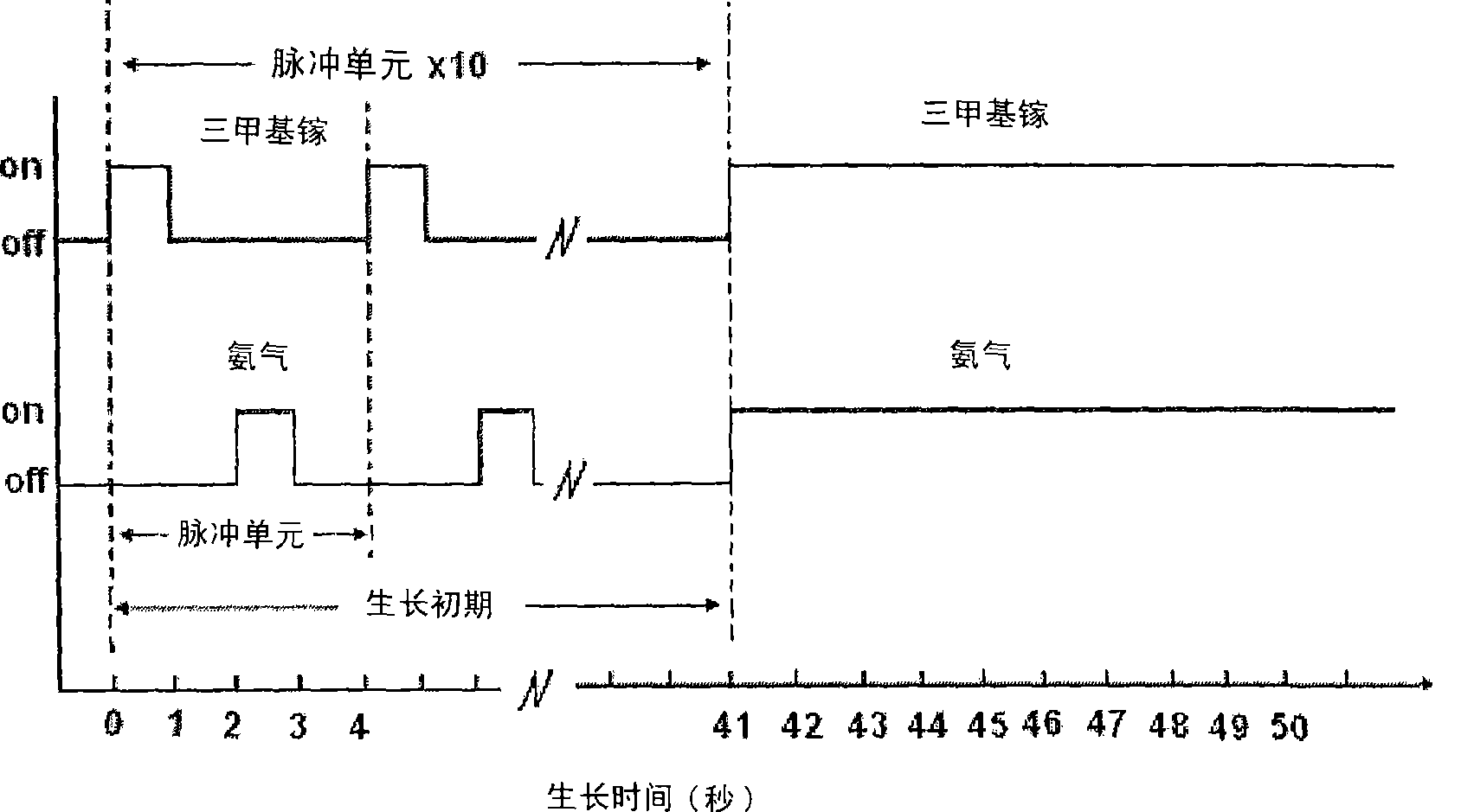
[0022] This embodiment provides a method for growing a gallium nitride thin film with high crystal quality on a sapphire substrate by using MOCVD equipment. The epitaxial equipment used is a commercial machine produced by VECOO Company of the United States, the model is D150. The V group source used is ammonia (NH3), the group III source material is trimethylgallium (TMG), the carrier gas is N2 and H2, and the flow rates of NH3 and TMG are 10 standard liters per minute (slm) and 100 micromoles, respectively. / min (μmol / m). The pressure of the reaction chamber is 150 Pascals (Pa).

[0023] The method for the epitaxial growth of the nitride thin film comprises the following steps:

[0024] First, put the 2-inch sapphire substrate into the MOCVD growth equipment.

[0025] Then raise the temperature of the sapphire substrate to 1100°C, and heat-treat the substrate for 10 minutes in a flowing H2 atmosphere to form an atomic step structure on the sapphire surface;

[0026] Then ...

Embodiment 2

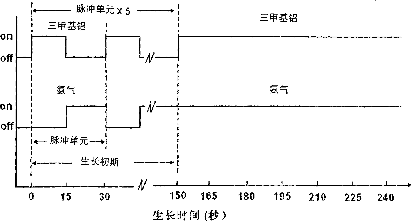
[0030] This embodiment provides a method for growing a high-quality aluminum nitride epitaxial layer on a sapphire substrate by using MOCVD equipment. The epitaxial equipment used is a commercial machine produced by VECOO Company of the United States, the model is D150. The source of group V used is ammonia (NH3), the source material of group III is trimethylaluminum (TMA), the carrier gas is N2 and H2, and the flow rates of NH3 and TMA are 0.5 standard liters per minute (slm) and 33 micromoles, respectively / min (μmol / m). The pressure of the reaction chamber is 75 Pascals (Pa).

[0031] The method for the epitaxial growth of the nitride thin film comprises the following steps:

[0032] First put the 2-inch sapphire substrate into the MOCVD growth equipment.

[0033] Then raise the temperature of the substrate to 1150°C, and heat-treat the substrate for 10 minutes in a flowing H2 atmosphere to form an atomic step structure on the surface;

[0034] In the subsequent growth ...

Embodiment 3

[0038] This embodiment provides a method for growing a high-quality aluminum gallium indium nitride (AlGaInN) epitaxial layer on a sapphire substrate by using MOCVD equipment. The epitaxial equipment used is a commercial machine produced by VECOO Company of the United States, the model is D150. The V group source used is ammonia (NH3), and the group III source materials are trimethylgallium (TMG), trimethylaluminum (TMA) and trimethylindium (TMI). The carrier gas is N2 and H2, and the pressure of the reaction chamber is 150 Pascal (Pa).

[0039] The method for the epitaxial growth of the nitride thin film comprises the following steps:

[0040] First, load the MOCVD growth equipment on the 2-inch sapphire substrate.

[0041] Then the temperature of the substrate was raised to 1100°C, and the substrate was heat-treated for 10 minutes in a flowing H2 atmosphere to form an atomic step structure on the surface;

[0042] Then lower the temperature of the substrate to 800°C, and ...


PUM


Abstract

The invention provides a method for epitaxial growth of nitride films, comprising the steps as follows: firstly, the temperature of a substrate is directly increased to the growth temperature of the nitride film; subsequently, during the early growth period, the input switch of ammonia gas (NH3) and III-cluster material is controlled by the computer program of growth equipment so that the ammonia gas (NH3) and III-cluster material are alternatively put into to a growth reaction chamber in pulse; during the process, a nucleation layer is formed on the surface of the substrate under the given duration, interval and pulse period; subsequently, the nitride film and device structure thereof with high crystal quality can grow on the nucleation layer. The method can simplify preparation process, reduces growth time, thereby reducing the growth cost and improving the growth efficiency. The method is beneficial for high crystal quality and for the growth of nitride film materials with low dislocation density.

Description

technical field [0001] The invention relates to the technical field of semiconductors, in particular to a method for epitaxial growth of a nitride thin film. The method can be used for the epitaxial growth of low dislocation density, high crystal quality nitride film and device structure material. Background technique [0002] Nitride (including gallium nitride, aluminum gallium nitride, aluminum nitride, indium gallium nitride, indium nitride, indium aluminum gallium nitride, etc.) is the third generation of direct energy gap wide bandgap semiconductors, and its bandgap width can be Adjustable between 0.7eV-3.39eV-6.28eV, covering the entire mid-infrared, visible and ultraviolet bands. Nitride can be used to make light-emitting devices, photodetection devices and laser devices from ultraviolet light to various colors of visible light and infrared light. At the same time, gallium nitride has high thermal and chemical stability, high electron saturation rate and carrier mob...

Claims


Application Information

Patent Timeline
IPC IPC(8): C30B25/02C30B29/38H01L21/205H01L33/00
Inventor 闫发旺高海永张扬张会肖李晋闽曾一平王国宏
Owner INST OF SEMICONDUCTORS - CHINESE ACAD OF SCI
Why Eureka
Try Eureka