Ultra-thin shielding film and circuit board capable of changing circuit impedance, and method for preparing same

A technology of circuit impedance and manufacturing method, applied in the fields of magnetic field/electric field shielding, printed circuit components, printed circuit secondary processing, etc., can solve the problems of easy breakage of metal layers, easy delamination, failure to shield and grounding, etc. , to achieve the effect of excellent bending performance, easy processing and impedance control

Active Publication Date: 2009-06-03
GUANGZHOU FANGBANG ELECTRONICS
View PDF1 Cites 33 Cited by
  • Summary
  • Abstract
  • Description
  • Claims
  • Application Information

AI Technical Summary

Problems solved by technology

The insulating layer of the outer layer is very thin, and the peel strength between the insulating layer and the shielding layer is low, and delamination is prone to occur in the process of multiple lamination processes; It is easy to break and cannot achieve the effect of shielding and grounding at the same time
On the other hand, since the conductor layer it forms is a solid metal layer, for flexible circuit board products, its function is only to play a shielding effect, which cannot meet the impedance function requirements of the product
For flexible circuit boards with impedance control, a thicker dielectric layer is required to use this shielding material to achieve the impedance value, which is costly and has a significant drop in bending resistance

Method used


Image

  • Ultra-thin shielding film and circuit board capable of changing circuit impedance, and method for preparing same
  • Ultra-thin shielding film and circuit board capable of changing circuit impedance, and method for preparing same
  • Ultra-thin shielding film and circuit board capable of changing circuit impedance, and method for preparing same

Examples


Embodiment 1

[0048] A method for manufacturing an extremely thin shielding film capable of changing circuit impedance, comprising the following steps:

[0049] 1), forming a peelable grid metal foil on the carrier:

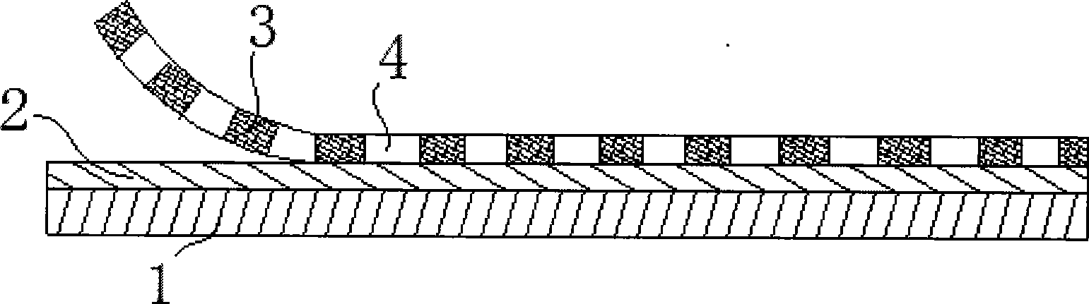
[0050] Such as figure 1 As shown, the step of forming the peelable mesh metal foil 3 on the carrier 1 is: pre-vacuum sputtering a layer of sputtered metal on the surface of the carrier 1 that can improve the peeling strength of copper, nickel or other metals from the carrier. Layer 3, then design the size of the carrier grid according to the impedance requirements of the product, and use methods such as drilling, punching, laser cutting or etching to form a grid of the same size on the carrier, and finally pass the roll shape on the sputtered metal layer A thin copper layer, a thin nickel layer, or a nickel-copper alloy layer is electroplated to form the meshed metal foil layer 3 . The meshed metal foil may include copper foil, nickel foil, aluminum foil and the like. The c...

Embodiment 2

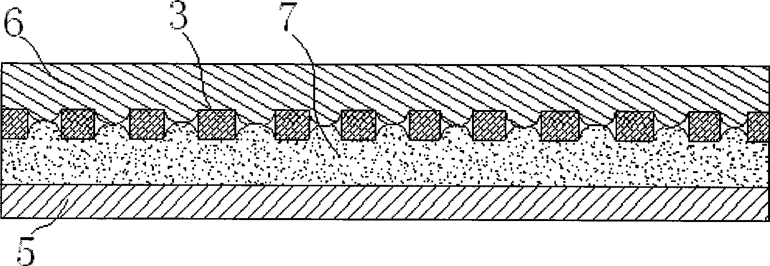
[0055] A method for manufacturing an ultra-thin shielding film capable of changing circuit impedance is based on the specific optimization of transferring the meshed metal foil to the insulating covering layer on the basis of the embodiments, including the following manufacturing steps:

[0056] 1), forming a peelable meshed metal foil on the carrier;

[0057] 2) Lay the outer shielding protective film transfer layer on the grid metal foil surface;

[0058] 3) Transfer the meshed metal foil on the carrier to the transfer layer of the outer shielding protective film, and remove the carrier.

[0059] 4), coating the insulating cover layer on the cover transfer layer, pre-curing; the described coating of the insulating cover layer on the transfer layer of the cover layer is on the transfer layer release film of the cover layer coated with silicone oil as required Coating the insulating covering layer, the insulating protective film has a certain initial tack, and the thickness i...

Embodiment 3

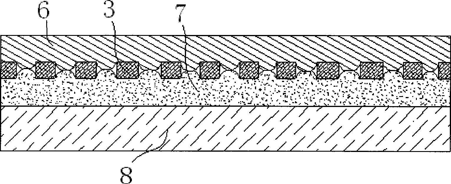
[0064] A method for manufacturing a printed circuit board covered with an extremely thin shielding film capable of changing circuit impedance, comprising the following manufacturing steps:

[0065] 1) cleaning and processing the surface of the single-sided circuit board substrate forming the circuit;

[0066] 2) An extremely thin shielding film that can change the impedance of the circuit is laminated on the front.

[0067] The substrate of the circuit board can be a uniform circuit formed on a single-sided substrate. The specific process can be directly attaching a film on the substrate, exposing, developing, and etching to form a uniform line, and then pressing the cover film.

[0068] In this embodiment, the ultra-thin shielding film that can change the impedance of the circuit is used to realize the impedance control of the single panel, which can replace the two-layer flexible circuit board. Generally, double-sided flexible copper clad laminates are used to realize the ...


PUM


Abstract

The invention provides an ultra-thin shielding film and a circuit board capable of changing circuit impedance, and a method for preparing same. The shielding film capable of changing the circuit impedance consists of an insulated coverage film layer, a metal foil layer, an anisotropic conductive adhesive layer and a protective release film layer; the metal foil layer is provided with meshes according to the impedance requirement design of the product and is arranged between the insulated coverage film layer and the anisotropic conductive adhesive layer; the surface of the anisotropic conductive adhesive layer is covered by the protective release film. The invention has the advantages that the ultra-thin layer of metal foil with a certain mesh dimension which is completely connected together is provided; the metal foil layer and the insulated layer have extremely high peeling strength, can durably bear heat impact and can be used for the multi-time pressing process of a soft / hard combination board; meanwhile, the thickness of a dielectric layer can be reduced and the aim of controlling the impedance can be achieved. Furthermore, the cost is low, the bending performance is excellent and the processing is easy.

Description

technical field [0001] The invention relates to the field of printed circuit boards and shielding films for printed circuit boards, in particular to an ultra-thin shielding film with high peel strength that can change circuit impedance, a circuit board and a manufacturing method thereof. Background technique [0002] Flexible printed circuit board, also known as flexible printed circuit board, or FPC, is a kind of flexible circuit board with high reliability and high flexibility made of polyimide or polyester film as the base material. printed circuit board. This kind of circuit board has good heat dissipation, can be bent, folded, curled, and can be moved and stretched freely in three-dimensional space. FPC can be used to reduce the volume, realize light weight, miniaturization and thinning, so as to realize the integration of component device and wire connection. FPC is widely used in industries such as electronic computers, communications, aerospace and home appliances....

Claims


Application Information

Patent Timeline
Patent Type & Authority Applications(China)
IPC IPC(8): H05K1/02H05K3/22H05K9/00
Inventor 苏陟
Owner GUANGZHOU FANGBANG ELECTRONICS
Why Eureka
Try Eureka