Terahertz GaN Gunn diode based on conducting type SiC substrate and manufacturing process thereof

A technology of Gunn diode and manufacturing method, which is applied in the field of microelectronics, can solve the problems of low output power, achieve the effects of improving heat dissipation, reducing parasitic series resistance, and reducing parasitic series resistance

Inactive Publication Date: 2009-07-08
XIDIAN UNIV
View PDF0 Cites 12 Cited by
  • Summary
  • Abstract
  • Description
  • Claims
  • Application Information

AI Technical Summary

Problems solved by technology

[0007] The purpose of the present invention is to provide a terahertz GaN Gunn diode structure and manufacturing method based on a conductive SiC substrate, so as to solve the problem of extremely low output power of the currently used GaAs-based Gunn devices in the THz frequency band. Provide good support for the further expansion of the THz field

Method used


Image

  • Terahertz GaN Gunn diode based on conducting type SiC substrate and manufacturing process thereof
  • Terahertz GaN Gunn diode based on conducting type SiC substrate and manufacturing process thereof
  • Terahertz GaN Gunn diode based on conducting type SiC substrate and manufacturing process thereof

Examples


Embodiment 1

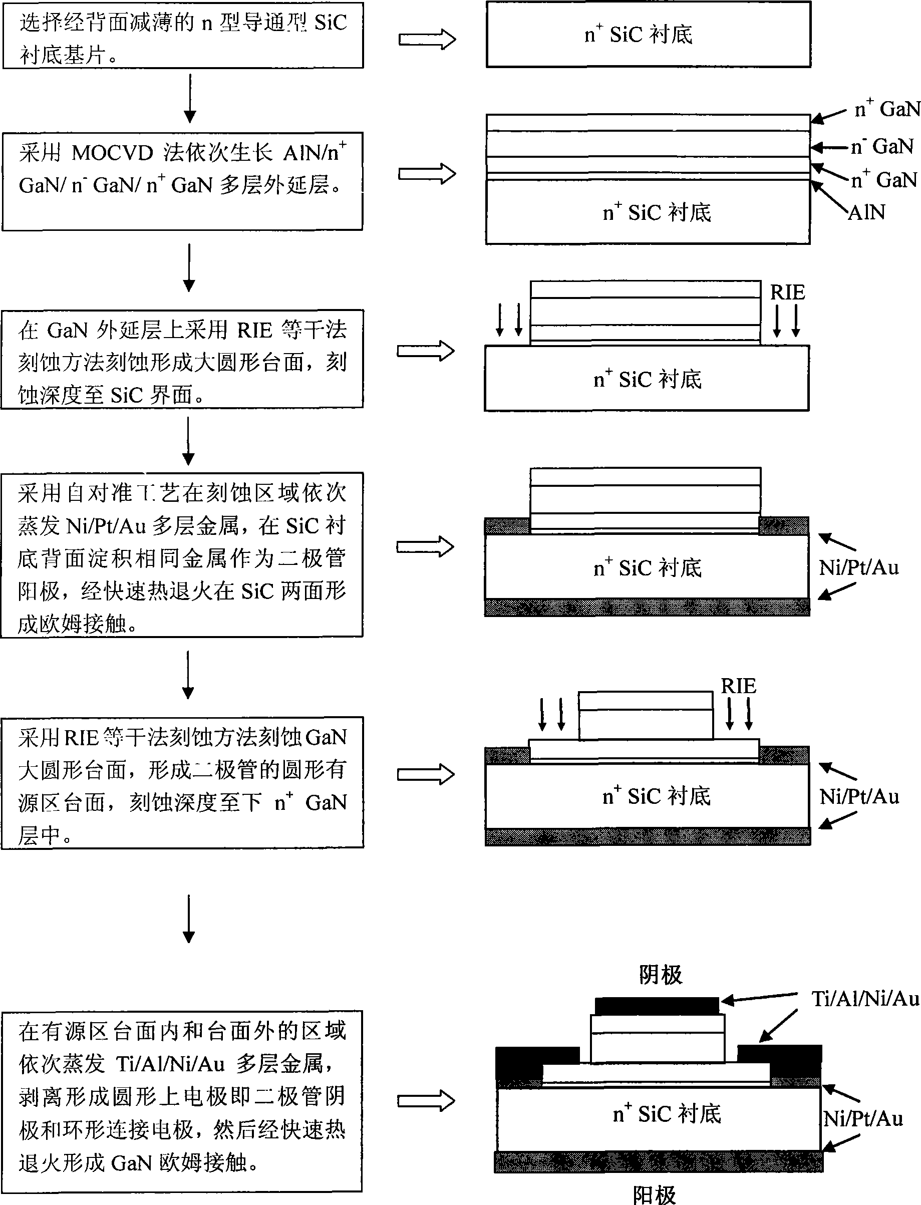
[0051] The invention manufactures a terahertz GaN Gunn diode based on a 2-inch n-type conduction type 4H-SiC substrate.

[0052] refer to image 3 Technological process, the production process of the present embodiment is as follows:

[0053] 1. Select a 2-inch 4H-SiC conduction-type n-type SiC substrate with a doping concentration of 5×10 18 cm -3 , the backside is thinned to a substrate thickness of 150 μm.

[0054] 2. Trimethylaluminum and high-purity ammonia are used as aluminum and nitrogen sources on MOCVD, and a low-temperature AlN nucleation layer is first grown on the SiC substrate at a temperature of about 600°C and a pressure of 40 Torr, with a thickness of 30nm.

[0055] 3. Using triethylgallium and high-purity ammonia gas as the source of gallium and nitrogen, and silane gas as the n-type doping source, control the temperature at 950°C and the pressure at 40 torr, and grow a layer of high-temperature n on the AlN nucleation layer. + GaN layer with a doping co...

Embodiment 2

[0068] The invention manufactures a GaN Gunn diode based on a 2-inch n-type conduction type 6H-SiC substrate and SiN passivation.

[0069] refer to image 3 Technological process, the production process of the present embodiment is as follows:

[0070] 1. Select a 2-inch 6H-SiC conduction-type n-type SiC substrate with a doping concentration of 5×10 18 cm -3 , the back side is thinned to a substrate thickness of 200 μm.

[0071] 2. Trimethylaluminum and high-purity ammonia are used as aluminum and nitrogen sources on MOCVD, and a low-temperature AlN nucleation layer is first grown on the SiC substrate at a temperature of about 600°C and a pressure of 40 torr, with a thickness of 50nm.

[0072] 3. Using triethylgallium and high-purity ammonia gas as the source of gallium and nitrogen, and silane gas as the source of n-type doping, control the temperature at 950°C and the pressure at 40 torr, and grow a layer of high-temperature n on the AlN nucleation layer. + GaN layer wi...

Embodiment 3

[0086] The invention manufactures a terahertz GaN Gunn diode based on a 3-inch n-type conduction type 4H-SiC substrate.

[0087] refer to image 3 Technological process, the production process of the present embodiment is as follows:

[0088] 1. Use a 3-inch 4H-SiC conduction-type n-type SiC substrate with a doping concentration of 5×10 18 cm -3 , the back side is thinned to a substrate thickness of 300 μm.

[0089] 2. Trimethylaluminum and high-purity ammonia are used as aluminum and nitrogen sources on MOCVD, and a low-temperature AlN nucleation layer is first grown on the SiC substrate at a temperature of about 600 °C and a pressure of 40 Torr, with a thickness of 40nm.

[0090] 3. Using triethylgallium and high-purity ammonia gas as the source of gallium and nitrogen, and silane gas as the n-type doping source, control the temperature at 950°C and the pressure at 40 torr, and grow a layer of high-temperature n on the AlN nucleation layer. + GaN layer with a doping con...


PUM

PropertyMeasurementUnit
Doping concentrationaaaaaaaaaa
Thicknessaaaaaaaaaa
Thicknessaaaaaaaaaa

Abstract

The invention discloses a THz GaN Gunn diode structure based on a conduction-type SiC substrate and the fabrication method thereof, which mainly solve the problem of extremely low output power of a GaAs-based THz Gunn device. The THz GaN Gunn diode comprises a SiC substrate layer, an AlN nucleation layer, and a GaN epitaxial layer, wherein the SiC substrate layer has an n-type conduction-type structure with a doping concentration of 5times10cm to ensure low-resistance conductivity; the low-temperature AlN nucleation layer has a thickness of 30 to 50 nm so that the dislocation density in the GaN epitaxial layer is reduced; the lower layer of the GaN epitaxial layer is a heavily-doped nGaN layer with a doping concentration of 5times10cm and a thickness of 1 mum; the intermediate layer is a lightly-doped NGaN layer with a doping concentration of 1times10cm and a thickness of 1 to 3 mum; and the upper layer is a heavily-doped nGaN layer with a doping concentration of 5times10cm and a thickness of 100 nm. Two etching steps are adopted in the entire fabrication of the device to realize the metallization with two different properties of SiC ohmic contact and GaN ohmic contact metallation, thereby reducing the parasitic series resistance. The THz GaN Gunn diode structure has the advantages of high output power and work frequency, and suits operation in THz bands.

Description

technical field [0001] The invention belongs to the field of microelectronics technology, and relates to semiconductor materials and device manufacturing technology, in particular to the structure and manufacturing method of a wide-bandgap semiconductor gallium nitride device, which can be used to make high-performance Gunn diodes suitable for terahertz frequency bands , can effectively improve the operating frequency and output power of the Gunn oscillator. Background technique [0002] The third-generation wide-bandgap semiconductor materials represented by silicon carbide SiC and gallium nitride GaN have large bandgap width, high critical field strength, high thermal conductivity, high carrier saturation rate, and high heterojunction interface two-dimensional Electron gas concentration and other excellent properties have attracted widespread attention in the field of microwave and millimeter wave high-power electronic devices. In recent years, with the development of ter...

Claims


Application Information

Patent Timeline
IPC IPC(8): H01L29/861H01L21/329
Inventor 杨林安郝跃张进城毛维冯倩
Owner XIDIAN UNIV
Why Eureka
Try Eureka