

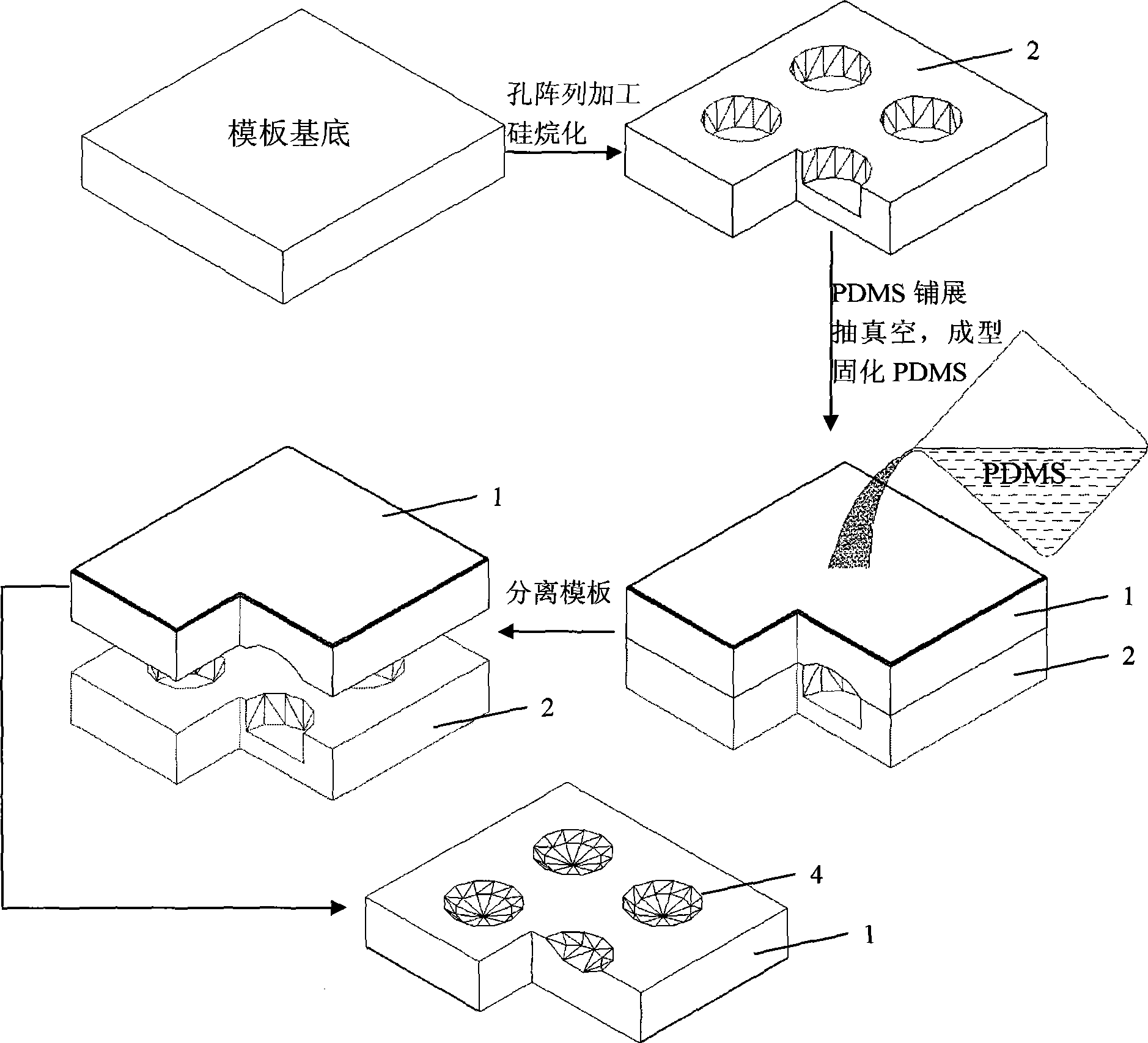
Preparation of micro-nano lens array
A lens array, micro-nano technology, applied in the direction of nanostructure manufacturing, lens, nanotechnology, etc., can solve the problems affecting the efficiency of the lens, and achieve the effect of expanding the scope of use, simple preparation process, and wide preparation range
- Summary
- Abstract
- Description
- Claims
- Application Information
AI Technical Summary
Problems solved by technology
Method used
Image

Examples
Embodiment 1
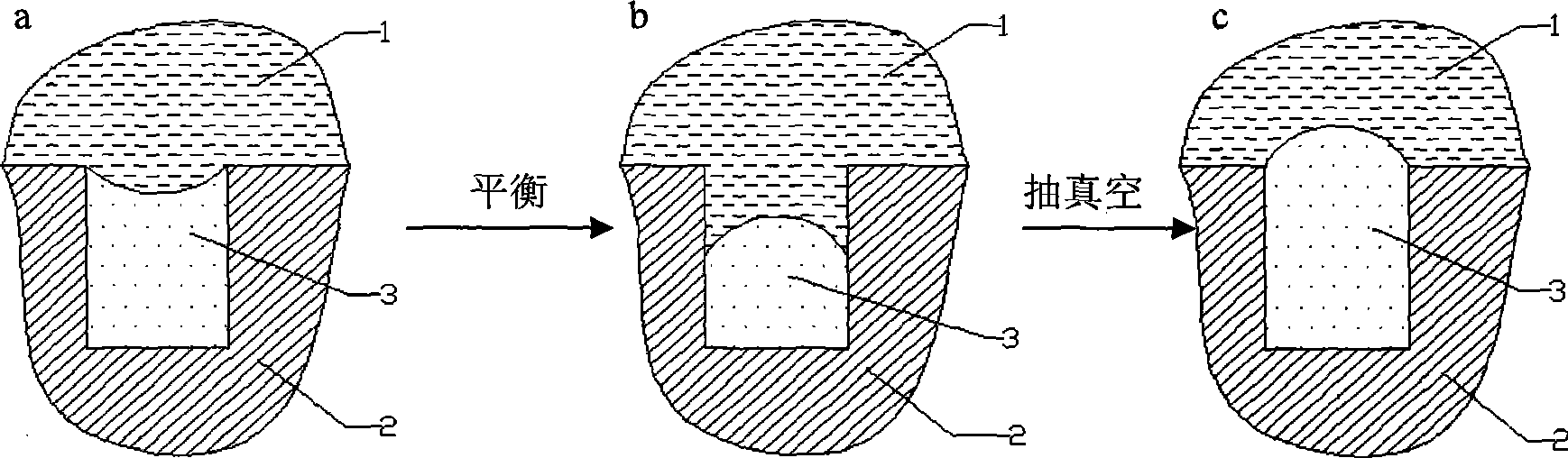
[0031] The template material is prepared, and a deep hole with a diameter of 300nm is processed by electron beam etching; after cleaning the prepared microhole array template 1, the template 1 is placed in a glass dish, and 1~ 3 μL of monosilane, then put the glass dish in a vacuum drying oven, evacuate to below 1000Pa and heat to 80-90°C, keep it warm for 60-70min, keep the vacuum to cool the system naturally, and take out the template when it reaches room temperature. After silanization treatment, the surface energy of the template surface is reduced, so that the liquid is not easy to flow to the bottom of the micropores; then the PDMS replica material is prepared according to the mass ratio of 10:1, and the mixed PDMS replica material is placed in vacuum drying In the drying box, vacuumize the drying box until the internal pressure is lower than 100Pa, and let it stand for 10 minutes for degassing. Then pour the treated liquid PDMS 1 onto the template 2; place the template ...
Embodiment 2
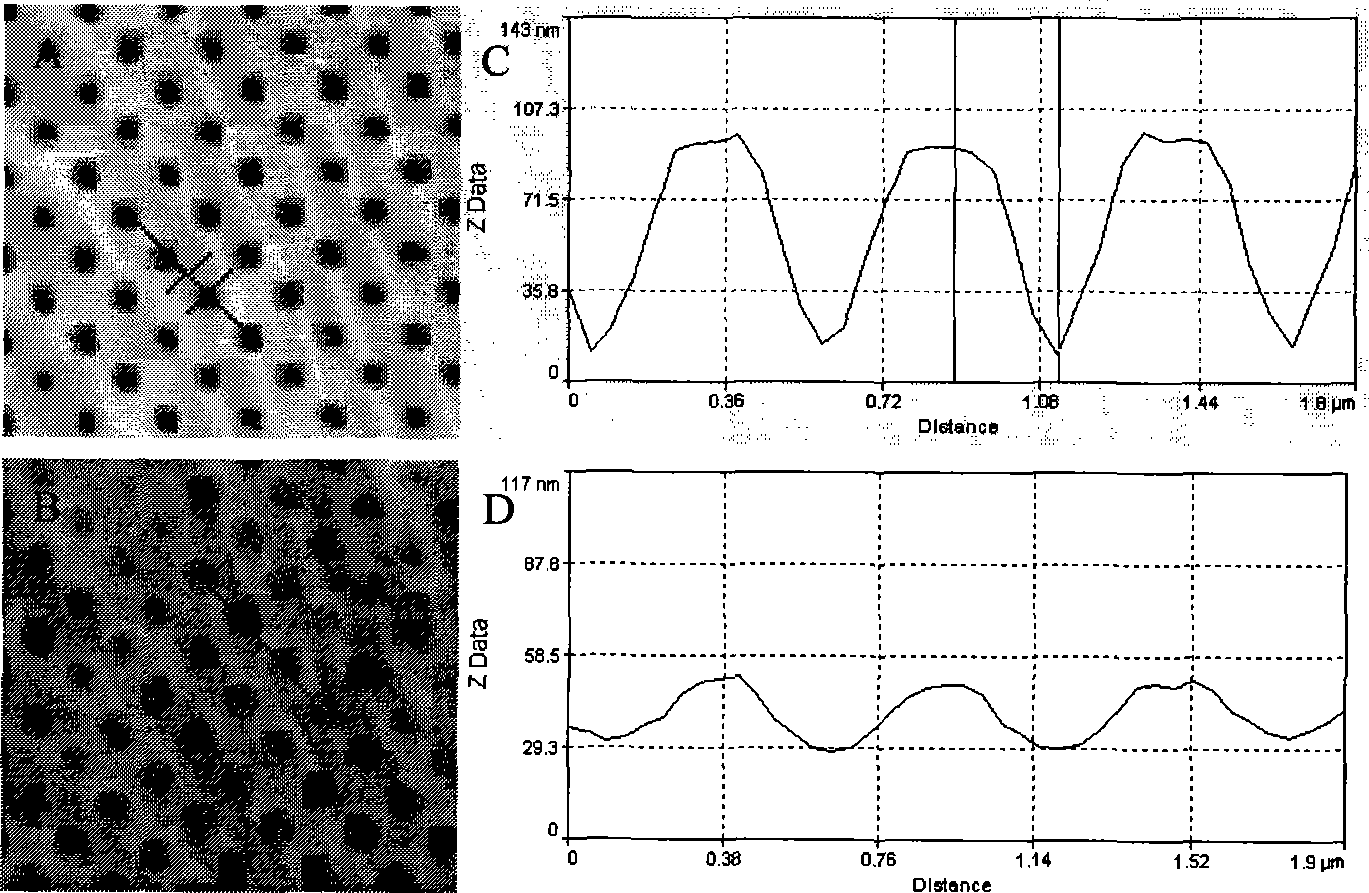
[0035] The implementation process is basically the same as that of Example 1, the difference is that the electron beam etching method is used to process a 50nm hole array on the silicon wafer; then carry out silanization treatment and spread the PDMS liquid on the surface of the template; send the template together with PDMS Into the vacuum drying oven, vacuum to below 100Pa. According to P 0 -P=2σ / r, the radius of curvature of the concave spherical surface obtained at this time is 400 nm, and the depth of the concave cavity is 1 nm.
Embodiment 3
[0037] The implementation process is the same as in Example 1, the difference is that a 1mm hole array is processed on a silicon wafer by a conventional method, and silanization is performed; PDMS is poured on the surface of the template; the template with PDMS liquid is sent into In a vacuum drying oven, vacuumize to 9.995×10 5 Pa and 1×10 5 Between Pa, a 1mm lens can be obtained by curing and molding.
[0038] Other microlens arrays with different scales can be prepared according to the above method by controlling the vacuum degree of the oven and using a microhole array template with a required diameter.
PUM
| Property | Measurement | Unit |
|---|---|---|
| diameter | aaaaa | aaaaa |
| diameter | aaaaa | aaaaa |
Abstract
Description
Claims
Application Information