Method for implementing image transfer on semiconductor material by anodised aluminum template

An anodized aluminum, pattern transfer technology, applied in semiconductor/solid-state device manufacturing, electrical components, circuits, etc., can solve the problems of low order and uniformity, inability to obtain high-performance devices, high process and equipment requirements, etc. Achieve the effects of simple production process and process, low preparation cost and high repeatability

Inactive Publication Date: 2009-08-05
INST OF SEMICONDUCTORS - CHINESE ACAD OF SCI
View PDF0 Cites 9 Cited by
  • Summary
  • Abstract
  • Description
  • Claims
  • Application Information

AI Technical Summary

Problems solved by technology

The traditional methods for preparing nanodot array systems mainly include electron beam lithography, molecular beam epitaxy, self-organized growth, chemical vapor deposition, etc. High, can not get good performance device

Method used


Image

  • Method for implementing image transfer on semiconductor material by anodised aluminum template
  • Method for implementing image transfer on semiconductor material by anodised aluminum template
  • Method for implementing image transfer on semiconductor material by anodised aluminum template

Examples


Embodiment

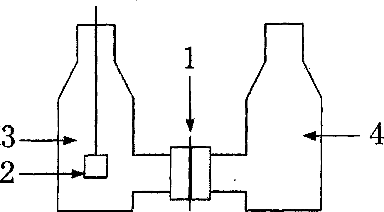
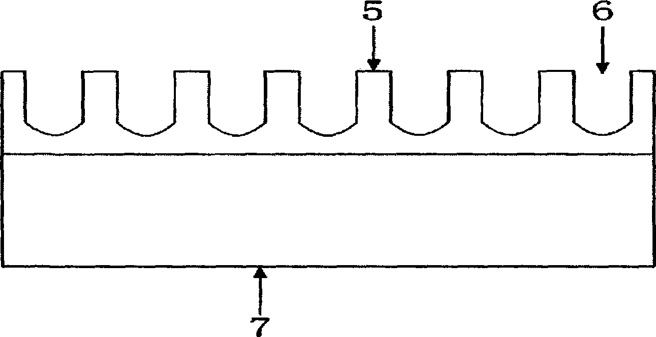
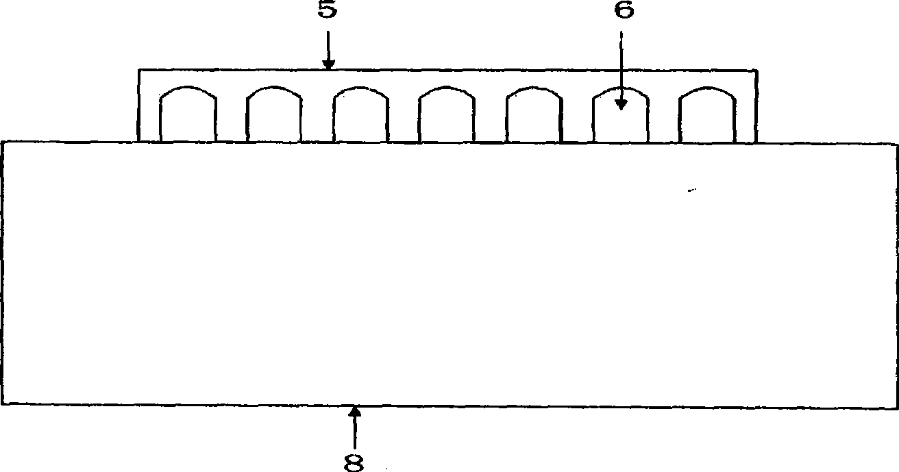
[0041] see figure 1 , figure 2 , image 3 , Figure 4 with Figure 5 In combination with specific examples, the process of utilizing the prepared anodized aluminum template to realize pattern transfer of small hole arrays on semiconductor materials will be further described in detail. Specifically include the following steps:

[0042] Step 1: Take an aluminum sheet 1, clean and polish;

[0043] Take an aluminum sheet 1 with a thickness of 100-500 microns and a purity of 99.99%. First soak in acetone for 1-5 hours to remove the oil on the surface of the aluminum sheet 1, then soak in a sodium hydroxide solution with a mass fraction of 4-6% at 60 degrees Celsius for 60-90 seconds to remove the natural oxidation on the surface of the aluminum sheet 1 After rinsing the membrane with deionized water, soak the aluminum sheet 1 in 300-400 g / L nitric acid solution for 3-5 minutes to remove the alkali film formed on the surface, and then rinse it with deionized water.

[0044]T...


PUM

PropertyMeasurementUnit
thicknessaaaaaaaaaa
thicknessaaaaaaaaaa
pore sizeaaaaaaaaaa

Abstract

A method using a porous alumina template for realizing the pattern transfer of semiconductor materials includes the following steps: 1. an aluminum sheet is gotten, and then cleaning and polishing are carried out; 2 a method for anodizing alumina is used for conducting a primary anodization and manufacturing a porous alumina film; 3. the porous alumina film which is formed at the primary anodization is dissolved; 4. the method for anodizing alumina is used for conducting a secondary anodization and manufacturing the porous alumina film; 5. the porous alumina film is separated from the aluminum sheet; 6. the porous alumina film is reversely affixed on a semiconductor material substrate and then dried; 7. annealing is carried out in an annealing furnace for improving the flatness of the film; 8. hole forming is carried out in phosphoric acid solution and the hole is put through in the two directions; 9. the porous alumina film is used as a mask for etching the semiconductor material with a drying method; and 10. the alumina film is dissolved in sodium hydroxide solution.

Description

technical field [0001] The invention belongs to the technical field of semiconductors, and relates to a method for realizing pattern transfer on semiconductor materials by using an anodized aluminum oxide template. Background technique [0002] Anodized aluminum film is prepared by anodic oxidation of aluminum sheet in acidic electrolyte by electrochemical technology, which can be traced back to the work of F.Keller et al. of American Aluminum Research Laboratory in 1953. The early application of alumina film mainly focused on the corrosion resistance, wear resistance, insulation and surface decoration of aluminum, and the corresponding research systems were mainly dense alumina film and disordered porous alumina film. After the 1990s, the research on quasi-one-dimensional nanomaterials gradually emerged. The characteristics of porous alumina templates just meet the requirements of one-dimensional nanosystems, and its research has developed by leaps and bounds. Now, porous ...

Claims


Application Information

Patent Timeline
Patent Type & Authority Applications(China)
IPC IPC(8): H01L21/308
Inventor 胡迪白安琪薛春来成步文王启明
Owner INST OF SEMICONDUCTORS - CHINESE ACAD OF SCI
Why Eureka
Try Eureka