Method for preparing transverse phase transition memory by using single-walled carbon nanotube as electrode

A single-walled carbon nanotube and phase-change memory technology, which is applied in the field of preparation of lateral phase-change memory, can solve the problems of high power consumption and excessive power consumption, and achieves low power consumption, small effective contact area, and reduced device operation. The effect of current and power consumption

Active Publication Date: 2009-09-02
SHANGHAI INST OF MICROSYSTEM & INFORMATION TECH CHINESE ACAD OF SCI
View PDF0 Cites 22 Cited by
  • Summary
  • Abstract
  • Description
  • Claims
  • Application Information

AI Technical Summary

Problems solved by technology

Through the test results, they found that due to the excessive power consumption caused by the leakage problem, the copper interconnection process cannot achieve the desired effect at

Method used


Image

  • Method for preparing transverse phase transition memory by using single-walled carbon nanotube as electrode
  • Method for preparing transverse phase transition memory by using single-walled carbon nanotube as electrode
  • Method for preparing transverse phase transition memory by using single-walled carbon nanotube as electrode

Examples


Embodiment Construction

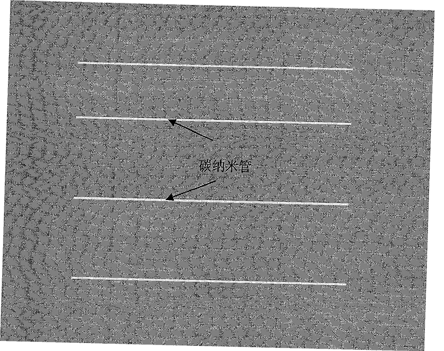
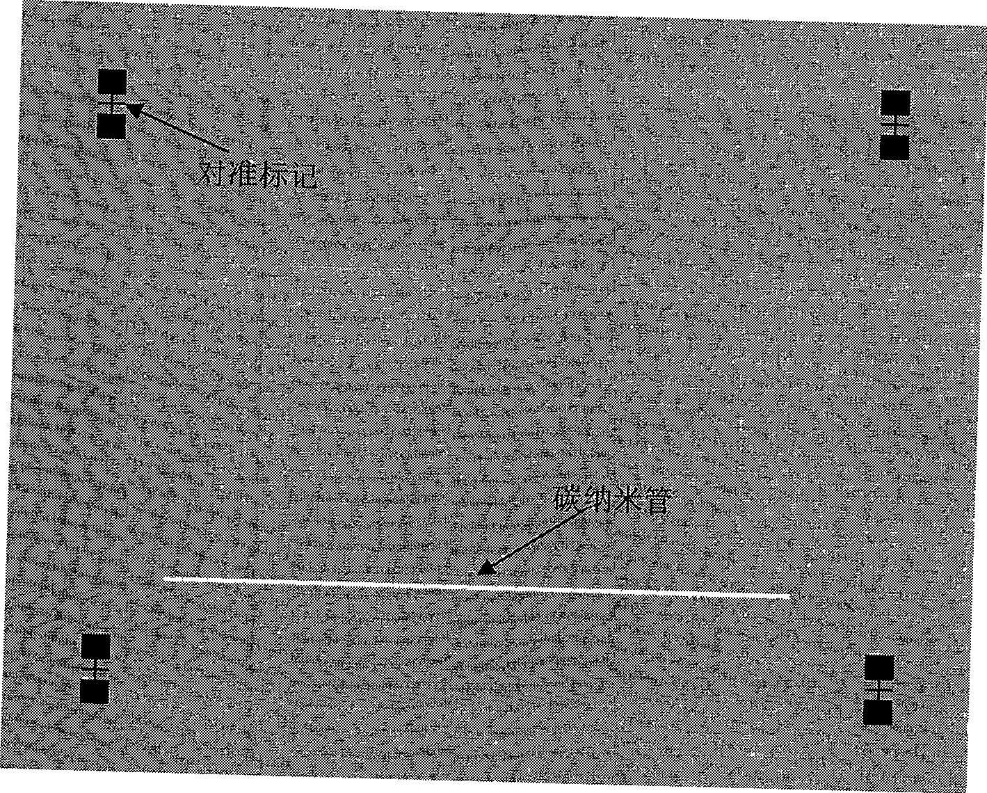
[0009] see Figure 1 to Figure 8 , the preparation method of the lateral phase change memory using single-walled carbon nanotubes as electrodes of the present invention mainly includes the following steps:

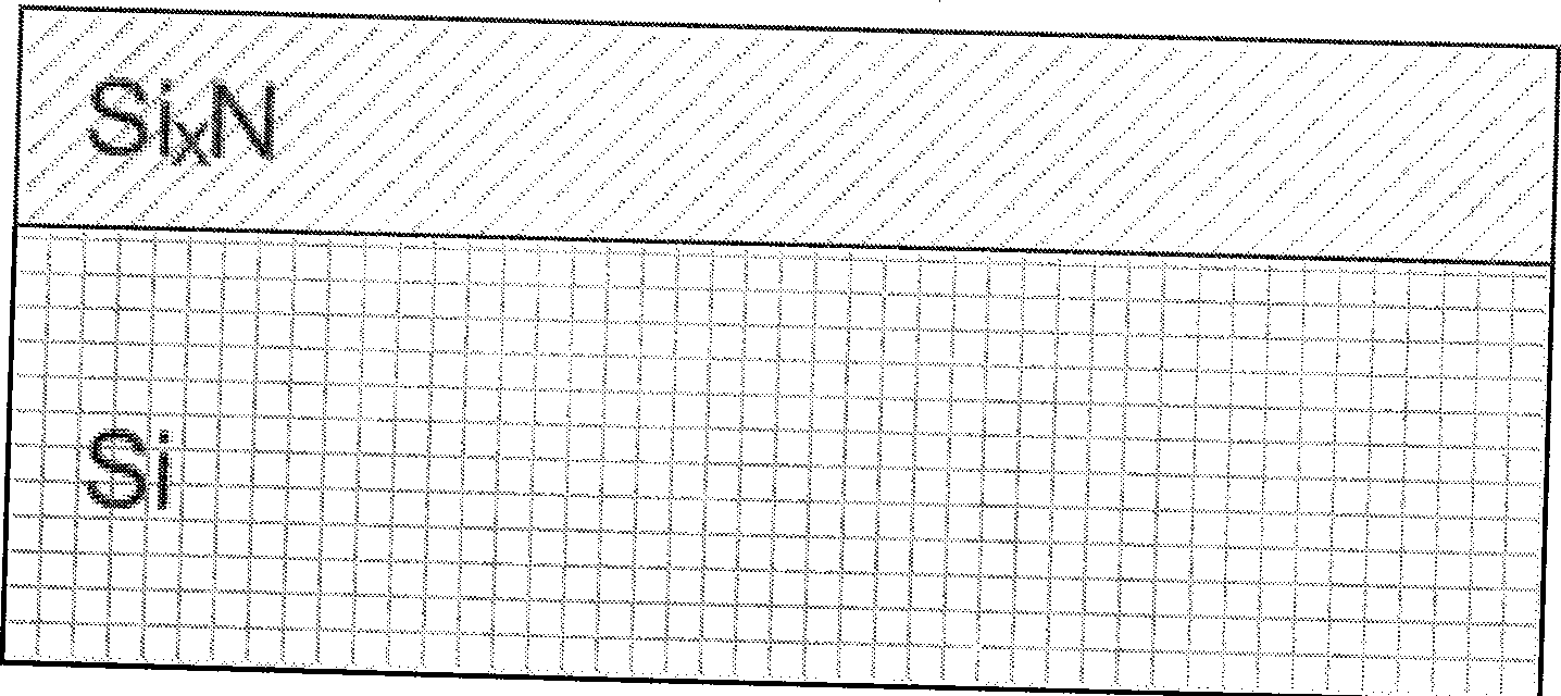
[0010] First, the semiconductor substrate is cleaned to remove dirt on the surface of the semiconductor substrate, and the semiconductor substrate is dried. In this embodiment, the semiconductor substrate material is silicon, and the steps of cleaning the silicon wafer are: (1) Cleaning the silicon wafer: 1# liquid: ammonia water: hydrogen peroxide: deionized water = 1:2:5, put the silicon wafer into Boil in 1# solution for 5 minutes, cool, rinse with deionized water for 3 minutes, and then blow dry with nitrogen. Main function: remove oil and large particles on the silicon surface. 2# solution: hydrochloric acid: hydrogen peroxide: deionized water = 1:2:5, put the silicon chip into 2# solution for cleaning, the method is the same as 1# solution, the main function is to r...


PUM

PropertyMeasurementUnit
Thicknessaaaaaaaaaa
Thicknessaaaaaaaaaa
Line widthaaaaaaaaaa

Abstract

The invention provides a method for preparing a transverse phase transition memory by using a single-walled carbon nanotube as an electrode. The method comprises the following steps: first, cleaning a semi-conductor substrate to remove stains on the surface of the substrate; depositing a medium layer on the substrate surface by a chemical vapor deposition method; preparing a transverse single walled carbon nanotube array on the medium layer by the chemical vapor deposition method; depositing a plurality of mask targets for photoetching and contact electrodes contacted with each carbon nanotube; etching the carbon nanotube by electron beam lithography and reactive ion etching to form an electrode couple array; depositing a phase transition material on the etched carbon nanotube between electrode couples by a magnetron sputtering method and electronic photetching technology; depositing an adiathermal protecting region on a structure with the deposited phase transition material by an ion beam deposition method and electron beam lithography; and preparing each test electrode, thereby forming the transverse phase transition memory with low power consumption.

Description

technical field [0001] The invention relates to a preparation method of a lateral phase-change memory, in particular to a preparation method of a lateral phase-change memory using single-walled carbon nanotubes as electrodes. Background technique [0002] Phase change memory (PRAM) is based on the reversible change of the resistance of the chalcogenide phase change material to realize the storage of information. Compared with the mainstream semiconductor storage technology currently on the market, PRAM has non-volatility, long cycle life, small component size, low power consumption, multi-level storage, high-speed reading, and radiation resistance (the ability to resist total dose is greater than 1Mrad), high and low temperature resistance (-55 ~ 125 ℃), anti-vibration, anti-electronic interference and simple manufacturing process, etc., not only can be widely used in civil microelectronics fields such as mobile phones, digital cameras, MP3 players, mobile memory cards, etc....

Claims


Application Information

Patent Timeline
IPC IPC(8): H01L21/822H01L21/28B82B3/00H01L45/00G11C11/56
Inventor 宋志棠吕士龙
Owner SHANGHAI INST OF MICROSYSTEM & INFORMATION TECH CHINESE ACAD OF SCI
Why Eureka
Try Eureka