PIN type nuclear battery and preparation method thereof
A nuclear battery and battery technology, applied in circuits, nuclear engineering, electrical components, etc., can solve the problems of inability to meet long-term power supply, small battery energy volume, etc., and achieve the effect of improving energy conversion efficiency, increasing energy density, and prolonging service life.
- Summary
- Abstract
- Description
- Claims
- Application Information
AI Technical Summary
Problems solved by technology
Method used
Image
Examples
Embodiment 1
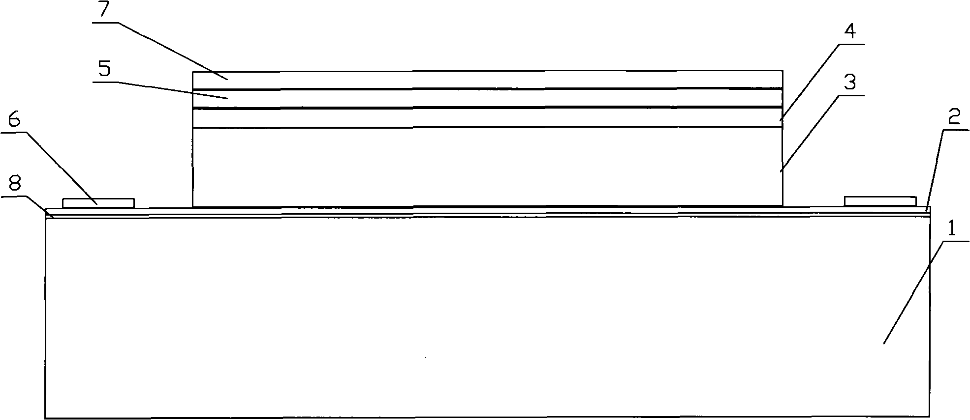
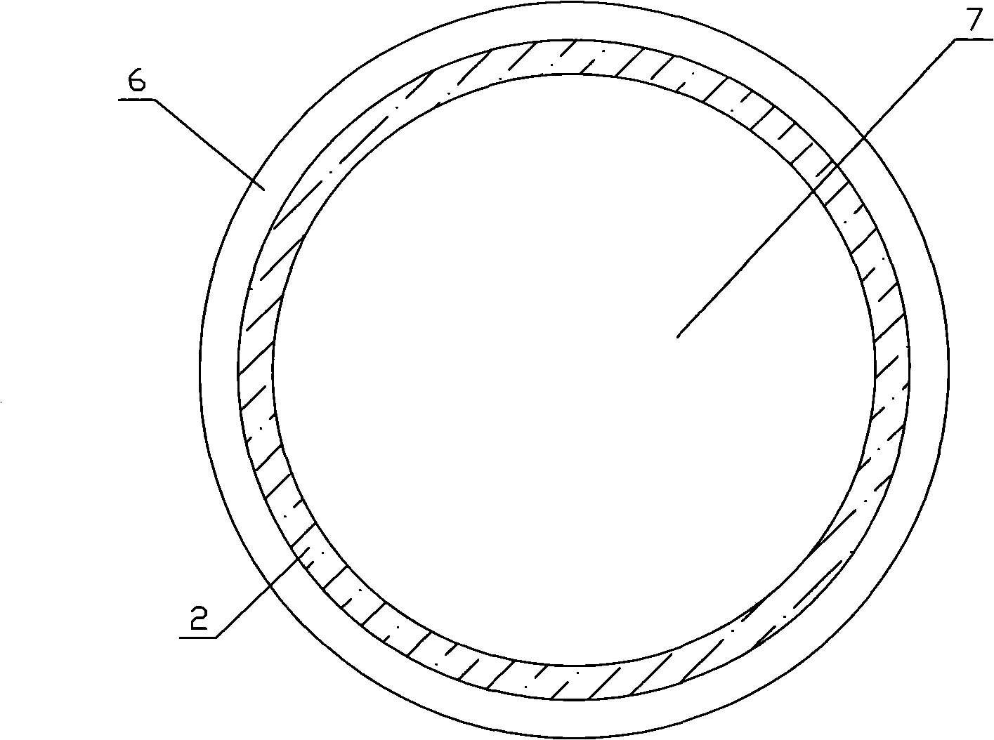
[0028] Such as figure 1 The shown schematic diagram of the structural axis section of an embodiment of the nuclear battery, first prepare the Al 2 o 3 Wafers, which can be purchased from the market to obtain single-side polished 2-inch C-side β-Al 2 o 3 The substrate 1 has a thickness of 300 μm.
[0029] Then carry out the PIN wafer growth process: use MOCVD epitaxial growth equipment, first Al 2 o 3 Substrate 1 is nitrided by passing through ammonia gas at 1100°C for about 2 minutes, then cooling down to 570°C, passing through trimethylgallium and ammonia gas to epitaxially form a gallium nitride (GaN) buffer layer 8 of about 20nm, and then raising the temperature to 1150°C Controlling the silicon doping concentration at 1×10 18 / cm 3 Under stable conditions, trimethylgallium, ammonia gas and silane are introduced to epitaxy n-GaN doped layer 2 of about 2 μm, and then the sample is taken out after cooling down to room temperature; Ammonia and metal gallium epitaxy 20μ...
Embodiment 2
[0032] Prepare Al first 2 o3 Wafers, which can be purchased from the market to obtain single-side polished 2-inch C-side β-Al 2 o 3 The substrate 1 has a thickness of 400 μm.
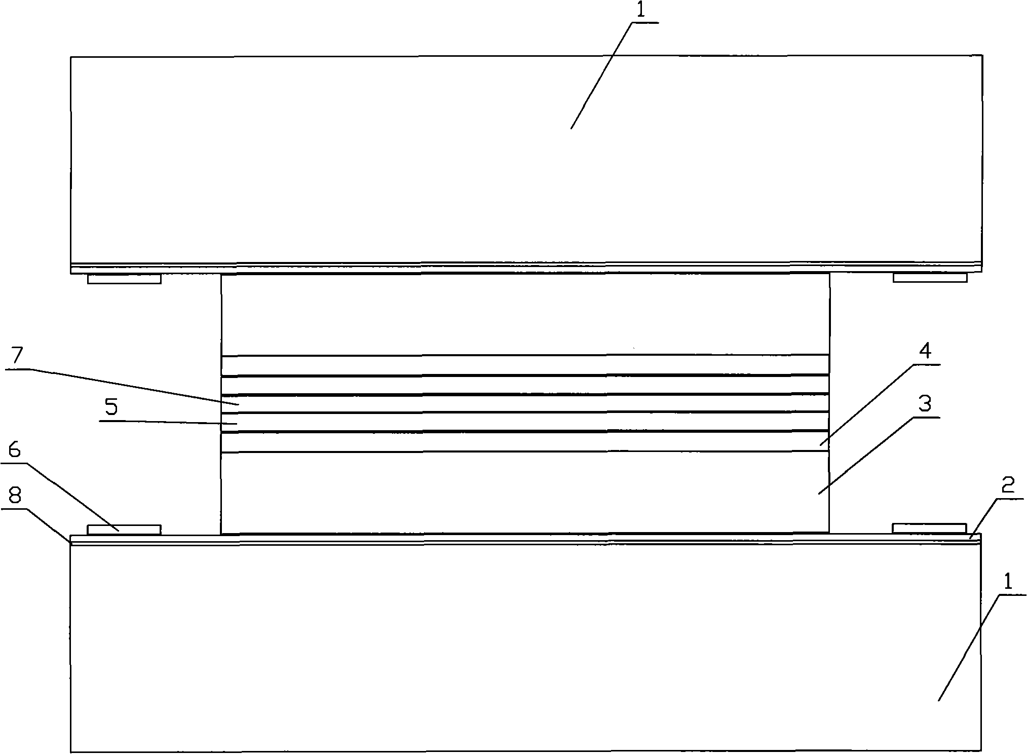
[0033] Then carry out the PIN wafer growth process: use MOCVD epitaxial growth equipment, first raise the temperature to 1150°C and control the silicon doping concentration at 1×10 19 / cm 3 Under stable conditions, trimethylgallium, ammonia gas and silane are introduced to epitaxy n-GaN doped layer 2 of about 2 μm, and then the sample is taken out after cooling down to room temperature; Ammonia and metal gallium epitaxy 20μm GaN insulating layer 3, then lowered to room temperature, took out the sample; put the sample back into the MOCVD system again, raised the temperature to 1070°C and controlled the magnesium doping concentration at 1×10 20 / cm 3 In a stable condition, trimethylgallium, ammonia gas and magnesocene are injected to epitaxially p-GaN doped layer 4 with a thickness of 17 nm.
[0034...
Embodiment 3
[0037] The preparation method is the same as that of the above two examples. The battery structure can be either the single structure of Example 1 or the composite structure of Example 2. The difference of this example is that the isotope layer 7 can also use nuclear waste strontium-90 , can also realize the preparation of high-efficiency radiovoltaic effect nuclear battery.
[0038] It should be noted that in all implementations including the above three examples, the total thickness of the p-type GaN doped layer and the p-type contact electrode cannot exceed 40nm (for the case described in Example 2, one side is used for calculation) , otherwise it will affect the conversion efficiency of the nuclear battery. Moreover, different nuclear batteries can be integrated in a certain way to obtain higher voltage or current nuclear batteries to meet the needs of different situations.
[0039] From the point of view of expanding applications, the micro-energy layout (each nuclear ce...
PUM
| Property | Measurement | Unit |
|---|---|---|
| Thickness | aaaaa | aaaaa |
| Thickness | aaaaa | aaaaa |
| Thickness | aaaaa | aaaaa |
Abstract
Description
Claims
Application Information


