Process for preparing back point-contact crystalline-silicon solar cells

A point-contact and solar cell technology on the back, applied in the field of solar cells, can solve problems such as difficult mass production, poor opening effect of the passivation layer on the back, difficult ohmic contact, etc., to achieve enhanced adhesion and good optical back reflection Performance, the effect of reducing the production cost

Inactive Publication Date: 2009-09-23
SUN YAT SEN UNIV
View PDF0 Cites 33 Cited by
  • Summary
  • Abstract
  • Description
  • Claims
  • Application Information

AI Technical Summary

Problems solved by technology

There are also reports on the opening of corrosive pastes by screen printing, but the effect of corrosive pastes on the opening of thick passivation layers is not very good; there are also direct printing of dotted metal pastes (such as aluminum pastes) On the passivat

Method used


Image

  • Process for preparing back point-contact crystalline-silicon solar cells
  • Process for preparing back point-contact crystalline-silicon solar cells
  • Process for preparing back point-contact crystalline-silicon solar cells

Examples


Embodiment 1

[0045] The preparation process of the rear point contact crystalline silicon solar cell provided in this embodiment, as attached figure 2 , 3 , 4, 5, 7 and 8, plate silicon dioxide 3 and silicon nitride 4 composite passivation film on the back of silicon chip 1, and adopt silicon paste screen printing on the composite passivation film with silicon paste with point contact pattern slurry layer 5, then use hydrofluoric acid solution to etch away the area not covered by the silicon paste layer in the composite passivation film, then screen print the aluminum paste layer 7 on the back of the silicon chip, and make the aluminum paste layer and the silicon paste layer by sintering A silicon-aluminum alloy layer 8 is formed on the contact surface, and the silicon-aluminum alloy layer 8 further enhances the adhesion of the aluminum layer. Because the thickness of the aluminum paste layer is relatively large, it can effectively prevent the aluminum paste from being applied to the SiO ...

Embodiment 2

[0059] as attached Figure 1-9 Shown: the preparation process of the rear point contact crystalline silicon solar cell provided in this embodiment includes the following steps:

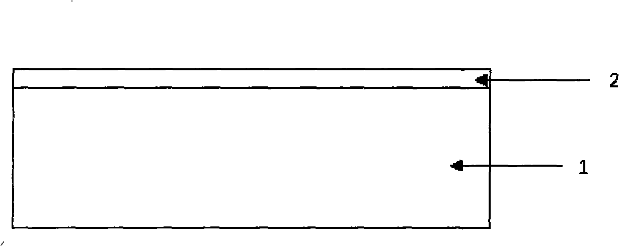
[0060] (1) forming an N-type layer 2 through diffusion on the front surface of the silicon wafer 1;

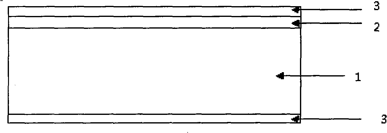
[0061] (2) forming a silicon dioxide layer 3 by thermal oxidation on both sides of the silicon wafer;

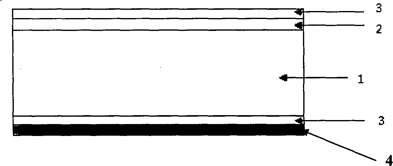
[0062] (3) coat one layer of silicon nitride 4 on the back side of the silicon wafer to form a composite passivation film of silicon dioxide and silicon nitride;

[0063] (4) On the composite passivation film, a silicon paste layer 5 with a point contact pattern is screen-printed with a silicon paste;

[0064] (5) using a chemical etching solution to etch away the area not covered by the silicon paste layer in the composite passivation film to form a point electrode contact hole, and simultaneously corrode the silicon dioxide layer on the front surface of the silicon wafer;

[0065] (6) coat the ...

Embodiment 3

[0080] Reference attached Figure 1-9 As shown, the preparation process of the rear point contact crystalline silicon solar cell provided in this embodiment includes the following steps:

[0081] (1) N-type layer 2 is formed by diffusion on both surfaces of silicon wafer 1;

[0082] (2) Remove the N-type layer on the back with acid or alkali, by first covering the N-type layer on the front, and removing the mask after removal;

[0083] (3) form a silicon dioxide layer 3 by thermal oxidation on both sides of the silicon wafer;

[0084] (4) coat a layer of silicon nitride 4 on the back side of the silicon wafer to form a composite passivation film of silicon dioxide and silicon nitride;

[0085] (5) On the composite passivation film, a silicon paste layer 5 with a point contact pattern is screen-printed with a silicon paste;

[0086] (6) using a chemical etching solution to etch away the area not covered by the silicon paste layer in the composite passivation film to form a po...


PUM

PropertyMeasurementUnit
Resistivityaaaaaaaaaa
Thicknessaaaaaaaaaa
Thicknessaaaaaaaaaa

Abstract

The invention discloses a process for preparing back point-contact crystalline-silicon solar cells. The process comprises the following steps: coating the back surface of a silicon wafer with a silicon dioxide and silicon nitride compound passivating film; screen-printing a silicon slurry layer with a point-contact pattern on the compound passivating film with silicon slurry; then, etching off the area which is not covered by the silicon slurry layer with a chemical etching solution; further screen-printing an aluminum slurry layer on the back surface of the silicon wafer; allowing the contact surface of the aluminum slurry layer and the silicon slurry layer to form a silicon-aluminum alloy layer by sintering; and finally, allowing the aluminum slurry and the silicon substrate on the back surface of the silicon wafer to form the local ohmic contact and the local aluminum back-surface field. The process can reduce the preparation cost and realize the industrial mass production more easily; and the prepared back point-contact electrode crystalline-silicon solar cell can form good back ohmic contact and local aluminum back-surface field, solve the problem that the resistance increases when the cells are connected in series caused by the point contact to a certain extent and maintain the good back-passivating effect and the optical back-reflecting property.

Description

technical field [0001] The invention belongs to the technical field of solar cells, and in particular relates to a preparation process of back point-contact crystalline silicon solar cells. Background technique [0002] In recent years, the output of crystalline silicon solar cells has grown rapidly, resulting in tight supply of silicon materials. For this reason, it is necessary to find a new process for preparing solar cells, which can reduce the cost on the one hand and improve the efficiency of the cell on the other hand. As the thickness of silicon wafers continues to decrease, the influence of the recombination rate on the back surface of silicon wafers on the efficiency of solar cells will become more and more prominent. The traditional aluminum back field process cannot meet the requirements of thin silicon wafer solar cells. However, point contact electrodes are considered to be a way to reduce the area of ​​the metal-semiconductor contact region and effectively r...

Claims


Application Information

Patent Timeline
IPC IPC(8): H01L31/18
CPCY02P70/50
Inventor 沈辉陈达明梁宗存
Owner SUN YAT SEN UNIV
Why Eureka
Try Eureka