Process for producing superconducting oxide material
A manufacturing method and oxide technology, applied in chemical instruments and methods, cable/conductor manufacturing, copper compounds, etc., can solve problems such as difficulty in orientation control, uniformity decline, etc., to achieve improved superconducting characteristics and high manufacturing efficiency , suitable for mass production
- Summary
- Abstract
- Description
- Claims
- Application Information
AI Technical Summary
Problems solved by technology
Method used
Image
Examples
Embodiment 1
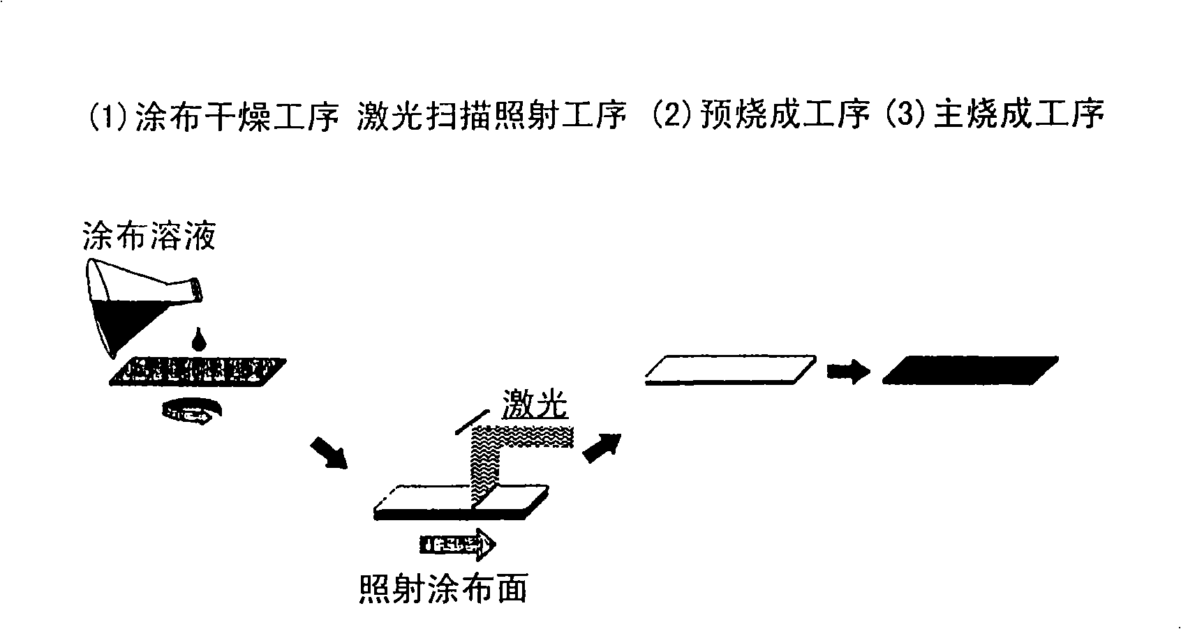
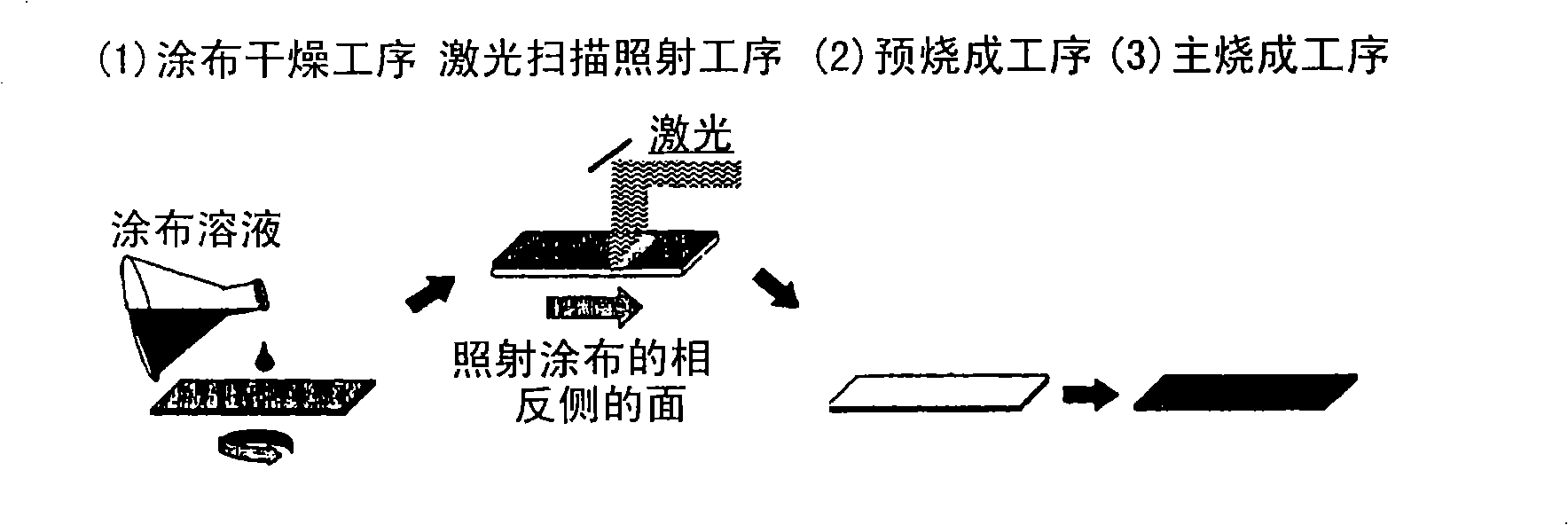
[0117] The coating solution Y1 was spin-coated on the substrate KC1 at 4000 rpm for 10 seconds, dried in a constant temperature bath at 130° C. to remove the solvent, and then irradiated with laser light H1 at room temperature. At this time, the intensity of the laser is set to 16.4mJ / cm 2 The laser scans in one direction, and irradiates with pulse numbers of 10,000, 20,000, 30,000, and 40,000 on one side.
[0118] Other irradiation conditions are as follows.
[0119] room temperature, atmosphere
[0120] Frequency: 100Hz
[0121] Overlap rate: 99%
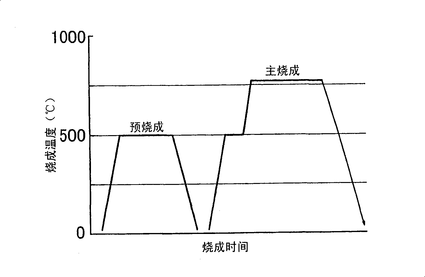
[0122] Next, the laser-irradiated sample was inserted into a muffle furnace previously kept at 500° C., kept at this temperature for 30 minutes, and then taken out. Then, main firing was performed in a quartz tubular furnace under the following conditions.
[0123] First, in the mixed gas flow of argon and oxygen with the oxygen partial pressure adjusted to 100ppm, the temperature was raised to 770°C at a rate of about 16°C p...
Embodiment 2
[0129] For comparison, except that laser irradiation is not carried out, other YBCO films with a film thickness of about 100nm made in the same manner as in Example 1, the Jc obtained by the induction method is within the detection limit (0.1MA / cm 2 )the following.
Embodiment 3
[0131] In addition to making the laser intensity 11mJ / cm 2 , the number of pulses is 500, and the amount of total energy is 5.5J / cm 2 In addition, other YBCO films with a film thickness of about 100 nm produced in the same manner as in Example 1 had a Jc of 1.1 MA / cm obtained by the induction method. 2 .
PUM
| Property | Measurement | Unit |
|---|---|---|
| thickness | aaaaa | aaaaa |
| strength | aaaaa | aaaaa |
| strength | aaaaa | aaaaa |
Abstract
Description
Claims
Application Information


