
Method for preparing bismuth nano wire array thermoelectric materials

A line array, thermoelectric material technology, applied in the field of thermoelectric materials and semiconductor material preparation, can solve the problems of inaccurate deposition time control, low filling rate of nanowire filling, and inability to control large area and single size, etc., to achieve emission stability Good, broad commercial application prospects, low cost effect

Inactive Publication Date: 2010-09-01
EAST CHINA NORMAL UNIV
View PDF0 Cites 0 Cited by
  • Summary
  • Abstract
  • Description
  • Claims
  • Application Information

AI Technical Summary

Problems solved by technology

The filling rate of filled nanowires prepared by direct current is low, and the nanowires have various sizes, which cannot control a single size in a large area
The pulse electrodeposition method does not control the deposition time accurately, and the deposition potential can only be deposited at two potentials.

Method used

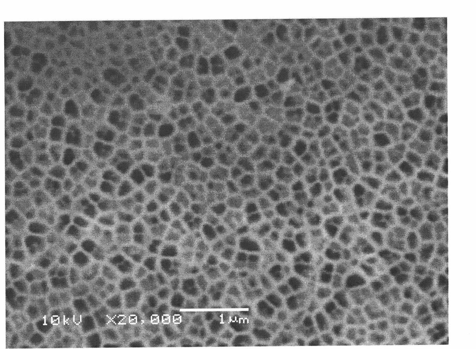
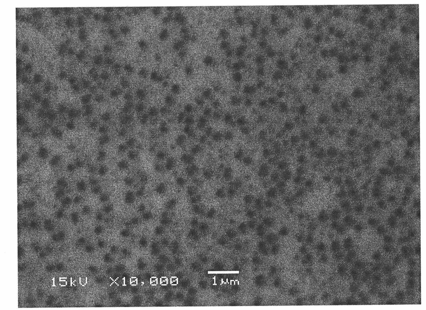
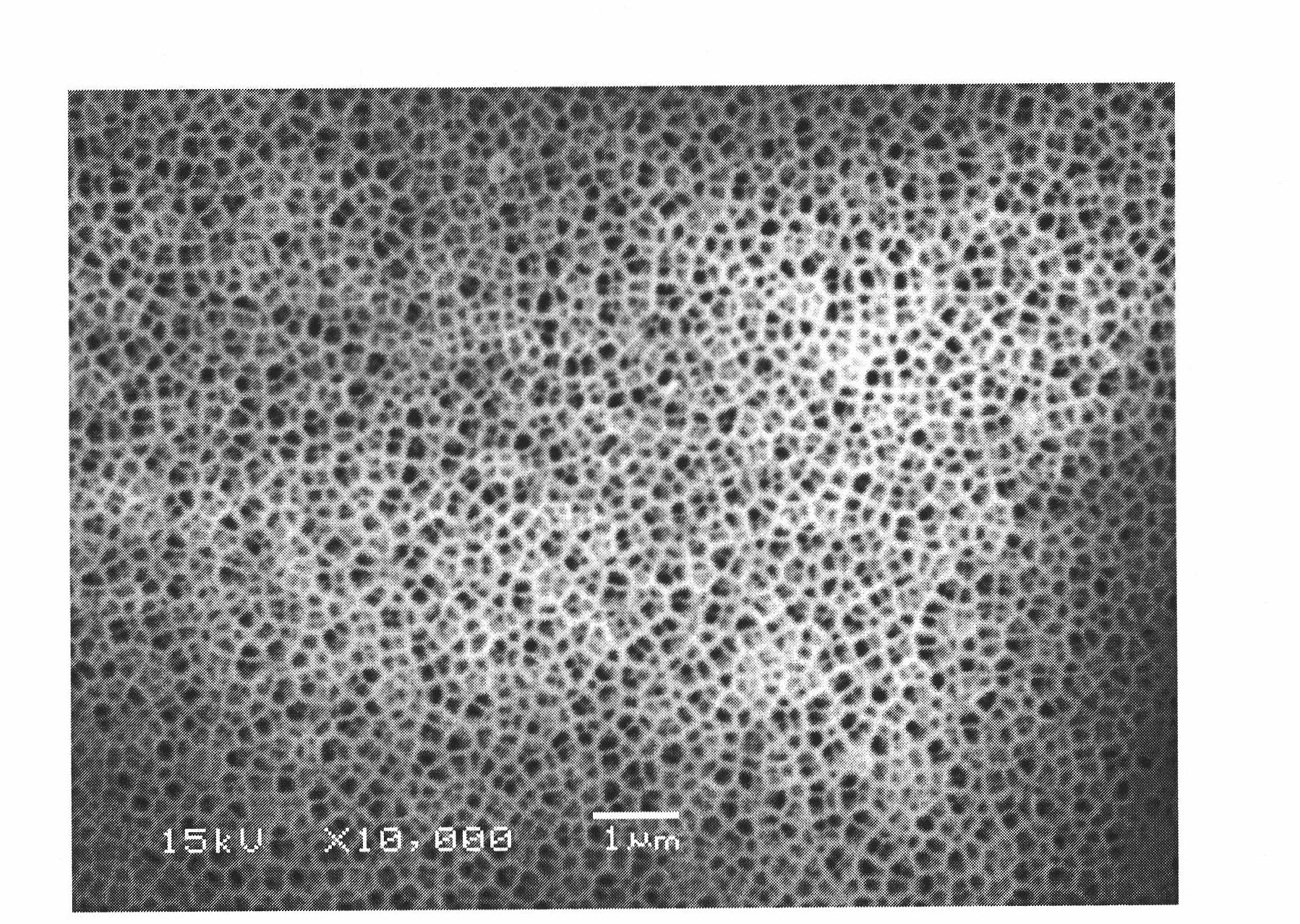

Image

  • Method for preparing bismuth nano wire array thermoelectric materials
  • Method for preparing bismuth nano wire array thermoelectric materials
  • Method for preparing bismuth nano wire array thermoelectric materials

Examples


Embodiment 1

[0018] a) Cut the alumina template into small pieces of 1cm×2cm, and then ultrasonically clean them in an alcohol solution.

[0019] b), prepare electrodeposition solution, the solution is made of 10g / l BiCl 3 , 50g / l tartaric acid, 95g / l glycerol and 50g / l NaCl solution, the pH value of the solution is adjusted to 0.9 with dilute hydrochloric acid.

[0020] c) Use CH1660C electrochemical workstation to electrodeposit alumina template, and select cyclic voltammetry, step 1: -1v step time 20ms; step 2: 0V step time 10ms; step 3: 1V The step time is 30ms as a cycle; the cycle step cycle, the deposition time is controlled for 120 minutes, and the electrochemical deposition software is closed to end the deposition.

[0021] d) After the electrodeposition is over, the template is taken out, placed in deionized water, ultrasonically cleaned, then placed in a NaOH (0.5 mol / l) solution, and allowed to stand for 30 minutes to remove the aluminum oxide film.

[0022] e) Distilling the solution ...


PUM

PropertyMeasurementUnit
pore sizeaaaaaaaaaa
thicknessaaaaaaaaaa
porosityaaaaaaaaaa

Abstract

The invention discloses a method for preparing bismuth nano wire array thermoelectric materials. The method is to take a high-purity BiCl3, glycerol and ammonia water solution as an electrodeposition solution, adopt electrochemical technology and utilize cyclic voltammetry to perform electrodeposition on an alumina template, and finally obtain the one-dimensional orderly Bi nano wire array thermoelectric materials with high thermoelectric conversion efficiency. The invention has simple preparation method and high filling rate; the maximum characteristic of the materials is that the materials can receive various forms of heat energy (including various types of radiant heat, solar energy, body temperature, heat generated in the system operation process, various types of waste heat and the like) from the environment and highly efficiently and directly convert the heat energy into electric energy which is then outputted; and due to the characteristics of the special high-density nano wirearray structure, oxidation resistance, high temperature resistance, high field emission current density, low turn-on field, good emission stability and the like, the application of the materials to field emission microelectronic devices as cathode materials can be realized and the materials have wide commercial application prospect.

Description

Technical field [0001] The invention relates to the preparation of thermoelectric materials and semiconductor materials, in particular to a method for preparing thermoelectric materials with periodically arranged Bi nanowires. technical background [0002] Bismuth is a typical semi-metallic material. Due to its highly anisotropic Fermi surface, very small effective mass of electrons, large carrier mean free path and semi-metal-semiconductor transition, it is used in thermoelectrics, sensors and giant magnets. Fields such as resistance have extremely broad application prospects. Theoretical research shows that due to the quantum confinement effect, the thermoelectric properties of bismuth will be significantly improved as the material dimensions decrease. In addition, as the diameter and orientation of the nanowires change, the electrical transport and thermoelectric properties of bismuth will be significantly different. Therefore, it is very important to explore the controlled ...

Claims


Application Information

Patent Timeline
Patent Type & Authority Patents(China)
IPC IPC(8): C25D3/54
Inventor 张志
Owner EAST CHINA NORMAL UNIV
Learn More