Structure and method of using step electrodes to realize nanometer beam drive and pressure resistance detection

A piezoresistive detection and ladder-shaped technology, which is applied in the manufacture of nanostructures, the measurement of the properties and forces of applied piezoresistive materials, nanotechnology, etc., can solve the problem of reducing the quality of nanobeams and increasing the complexity of the process by protecting the oxide layer of the gate, etc. problems, to avoid the influence of stress distribution and quality factor, to avoid protection, and to simplify the process

Inactive Publication Date: 2009-10-28
SHANGHAI INST OF MICROSYSTEM & INFORMATION TECH CHINESE ACAD OF SCI
View PDF1 Cites 8 Cited by
  • Summary
  • Abstract
  • Description
  • Claims
  • Application Information

AI Technical Summary

Problems solved by technology

However, the disadvantage of this structure is that the gate oxide layer and metal gate of the MOS capacitor will reduce the quality factor of the nanobeam; at the same time, because the thickness of the MOS capacitor is greater than the thickness of other parts of t

Method used


Image

  • Structure and method of using step electrodes to realize nanometer beam drive and pressure resistance detection
  • Structure and method of using step electrodes to realize nanometer beam drive and pressure resistance detection
  • Structure and method of using step electrodes to realize nanometer beam drive and pressure resistance detection

Examples


Embodiment 1

[0024] Embodiment 1 The manufacturing process steps of the double-terminal fixed-supported nano-beam driving and piezoresistive detection structure provided by the present invention are as follows:

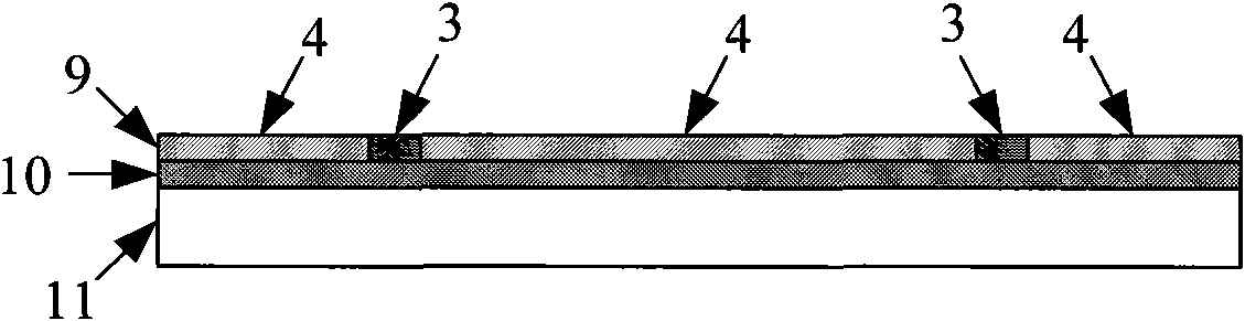
[0025] (1) On the top silicon layer of the SOI silicon wafer, a light boron doped region and a rich boron doped region are fabricated by ion implantation. Such as figure 2 As shown, in the figure, a boron-lean region 3 and a boron-rich region 4 are fabricated on the top layer silicon 9 of the SOI silicon wafer. Under the top layer of silicon 9 are buried layer silicon dioxide 10 and substrate silicon 11 .

[0026](2) Thermally oxidize the SOI silicon wafer, and thermally grow a silicon oxide layer on the top layer of silicon, and thermal oxidation will reduce the thickness of the top layer of silicon. The thermal oxidation time is controlled to reduce the top silicon thickness to the target thickness of the nanobeams. Remove the thermal oxide layer on the surface.

[0027] (3)...

Embodiment 2

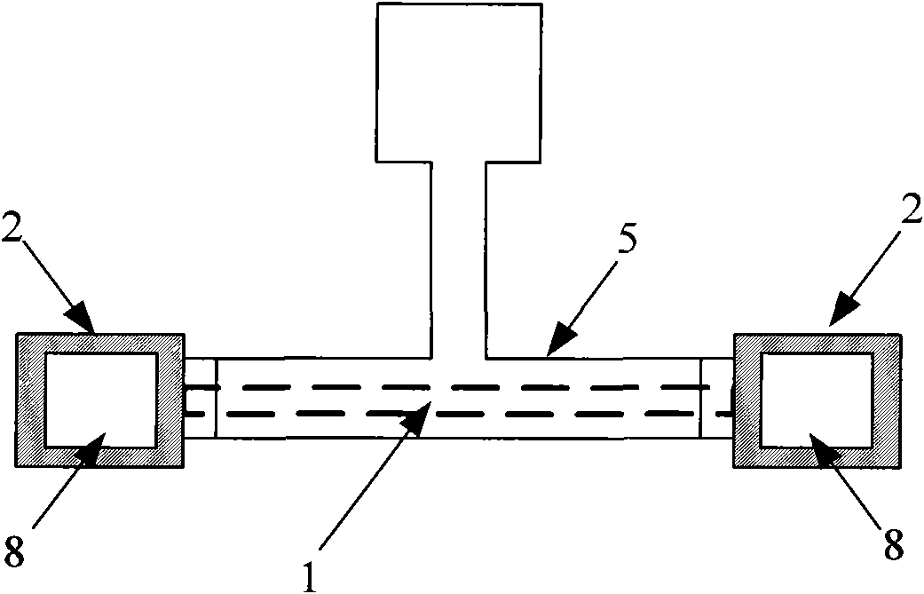
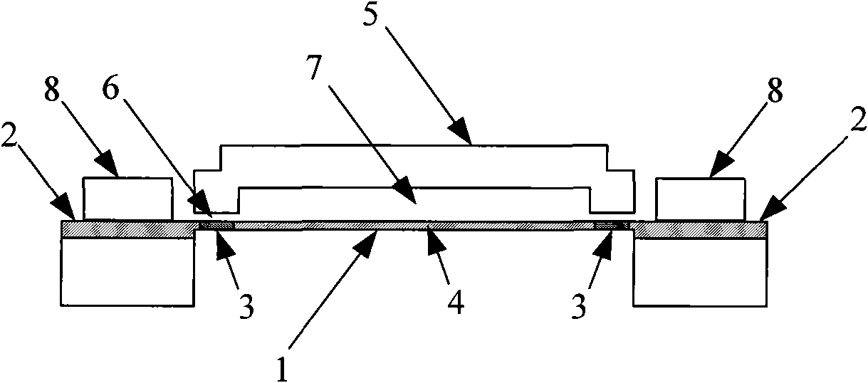
[0034] FIG. 7 is a structural schematic diagram of the electrostatic drive of the nanometer-thick cantilever and the piezoresistive detection of the MIS capacitive substrate by using stepped electrodes. Fig. 7(a) is a top view, and Fig. 7(b) is a top view of the nanobeam structure after removing the stepped electrodes. The nanobeams are fabricated on N-type silicon wafers, that is, the initial doping type of the nanobeams is N-type. When the cantilever nanobeam moves up and down, the stress maximum point appears at the end point, so the force sensitive resistor is made at the end point. Due to the characteristics of the cantilever beam structure, the force sensitive resistor is arranged in a state perpendicular to the nanobeam, and the force sensitive resistor is doped with light boron. The ladder-shaped electrode and the lightly boron-doped region on the nanobeam form a MIS capacitor structure, and the densely boron-doped region on the nanobeam is used for electrostatic driv...


PUM

PropertyMeasurementUnit
Doping concentrationaaaaaaaaaa

Abstract

The invention relates to a structure and a method of using step electrodes to realize nanometer beam drive and pressure resistance detection, which are characterized in that a metal electrode on the upper part of the nanometer beam is of step-shape; the clearance between the two ends of the electrode and the nanometer beam is smaller than 100 nanometers; while the electrode clearance in the middlepart is between 1 and 2 microns. An MIS capacitor structure is formed between the two ends of the step electrode and the nanometer beam. When the voltage between the step electrode and the nanometerbeam exceeds the threshold voltage of the MIS capacitor, a space charge area below the MIS capacitor achieves the maximum value; and the resistance under the space charge area is only a stress function, which can be used for detecting the pressure resistance of the nanometer beam. The central part of the step electrode has small effect on the resistance value of the nanometer beam due to the largeclearance; the drive efficiency of the central part to the nanometer beam is high; and the central part is used for realizing static drive on the nanometer beam.

Description

technical field [0001] The present invention relates to the principle and structure of a nano-beam and a ladder-shaped driving electrode for electrostatically driven piezoresistive detection, and more precisely relates to a structure of a nano-beam and a ladder-shaped driving electrode. While the beam is electrostatically driven, a space charge region is induced on the surface of the nanobeam, and the part under the space charge region of the nanobeam is used as a force sensitive resistor to realize piezoresistive detection. It belongs to the field of micro / nano fabrication. Background technique [0002] Nano Electro Mechanical System (NEMS) is the development of Micro Electro Mechanical System (MEMS) and is an important part of nanotechnology. Due to the use of nanoscale effects such as surface effects and scale effects of nanoscale structures, new devices can be realized, and the performance of existing devices can be significantly improved (K.L.Ekinci, M.L.Roukes. Nanoel...

Claims


Application Information

Patent Timeline
IPC IPC(8): B82B1/00B82B3/00G01L1/18
Inventor 杨恒吴燕红成海涛戴斌李昕欣王跃林
Owner SHANGHAI INST OF MICROSYSTEM & INFORMATION TECH CHINESE ACAD OF SCI
Why Eureka
Try Eureka