Thermo-optical infrared detector and preparation method thereof

An infrared detector and manufacturing method technology, applied in chemical instruments and methods, optical radiation measurement, radiation pyrometry, etc., can solve the problems of not designing an infrared absorption layer, not realizing vacuum packaging of devices, and limiting pixel thermal insulation performance, etc. , to achieve the effect of easy batch production, low production difficulty, and easy miniaturization

Active Publication Date: 2009-10-28
SHANGHAI INST OF MICROSYSTEM & INFORMATION TECH CHINESE ACAD OF SCI
View PDF0 Cites 21 Cited by
  • Summary
  • Abstract
  • Description
  • Claims
  • Application Information

AI Technical Summary

Problems solved by technology

In this scheme, the height of the heat-insulating columns supporting the pixels is determined by the thickness of the sacrificial layer. Generally speaking, the thickness of the sacrificial layer is usually only a few microns thick, resulting in the low height of the heat-insulating columns of the pixels, which limits the thermal insulation performance of the pixels. This is also one of the main reasons why the noise equivalent temperature difference of the TO-IRD they made is not high; there is no special infrared absorption layer designed, and the absorption rate of infrared radiation is low; Realize vacuum packaging of devices

Method used


Image

  • Thermo-optical infrared detector and preparation method thereof
  • Thermo-optical infrared detector and preparation method thereof
  • Thermo-optical infrared detector and preparation method thereof

Examples


Embodiment 1

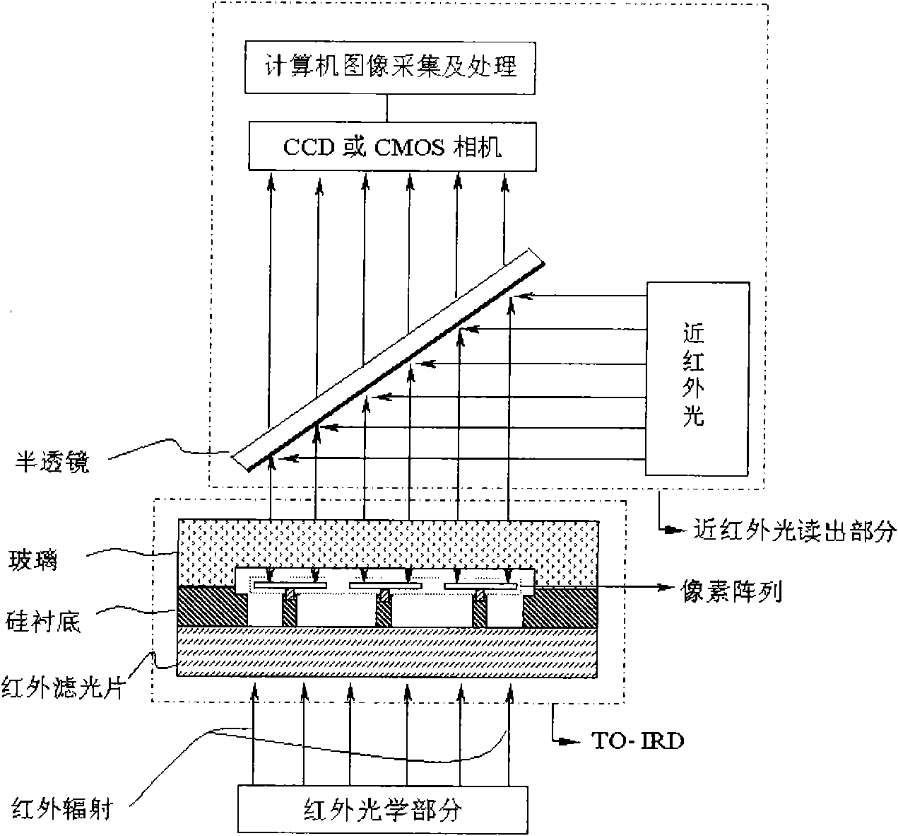
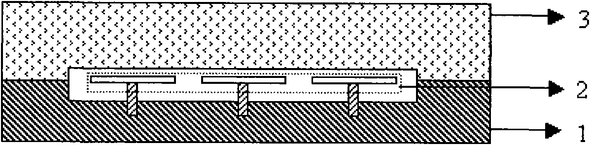
[0042] As shown in Figure 2, the provided TO-IRD consists of a silicon substrate 1, a pixel array 2, and a glass 3; the silicon substrate 1 not only acts as a substrate and a heat sink, but also acts as an infrared filter, while No special infrared filter is needed; the pixel array 2 is fabricated on the silicon substrate 1 , and the glass 3 and the silicon substrate 1 are connected by bonding to realize vacuum packaging of the pixel array 2 .

[0043] Combine below Figure 5 The process flow of this embodiment is described in detail, and the present invention is further described.

[0044] (1) Using photoresist or silicon oxide as a mask, etch the silicon substrate 1 by deep reactive ion etching (DRIE) or other methods to form a deep groove 6, the depth of the deep groove 6 is greater than 10 μm, and remove the mask layer, Such as Figure 5 as shown in a;

[0045] (2) The method of thermal oxidation or thermal oxidation, polysilicon growth, and secondary thermal ...

Embodiment 2

[0053] As shown in Figure 3, the provided TO-IRD consists of a silicon substrate 1, a pixel array 2, a glass 3 and an infrared filter 4; the silicon substrate 1 acts as a substrate and a heat sink; the pixel array 2 is fabricated on the silicon substrate 1, and the glass 3 is connected to the silicon substrate 1 by bonding, which improves the mechanical strength of the device, and the vacuum packaging of the pixel array 2 is realized by bonding the infrared filter 4 under the silicon substrate 1 .

[0054] Combine below Figure 6 The process flow of this embodiment is described in detail, and the present invention is further described.

[0055] (1) repeat the technological process of embodiment 1 (as Figure 5 shown in a-h), the process results are as follows Figure 6 as shown in a;

[0056] (2) Etch the silicon substrate 1 by deep reactive ion etching (DRIE) or other methods, and remove the silicon substrate below the pixel (except for the thermal insulation co...

Embodiment 3

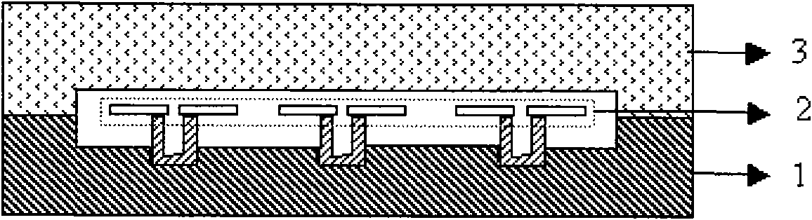
[0059] As shown in Figure 2(b), the provided TO-IRD consists of a silicon substrate 1, a pixel array 2, and a glass 3; the silicon substrate 1 not only acts as a substrate and a heat sink, but also acts as an infrared filter. function without special infrared filter; the pixel array 2 is fabricated on the silicon substrate 1, and the glass 3 and the silicon substrate 1 are connected by bonding to realize the vacuum packaging of the pixel array 2. The difference from Embodiment 1 is that in order to further improve the heat insulation performance of the pixel, the heat insulation column in this embodiment is hollow.

[0060] Combine below Figure 7 The process flow of this embodiment is described in detail, and the present invention is further described.

[0061] (1) Using photoresist or silicon oxide as a mask, etch the silicon substrate 1 by deep reactive ion etching (DRIE) or other methods to form a deep groove 6, the depth of the deep groove 6 is greater than 10 μm,...


PUM

PropertyMeasurementUnit
heightaaaaaaaaaa
thicknessaaaaaaaaaa

Abstract

The invention relates to a thermo-optical infrared detector and a preparation method thereof, and is characterized in that the infrared detector consists of a silicon substrate, a pixel array arranged on the silicon substrate and a glass bonded with the silicon substrate; alternatively, the infrared detector consists of a silicon substrate, a pixel array arranged on the silicon substrate, a glass bonded with the silicon substrate and an infrared filter bonded with the silicon substrate. In the TO-IRD, a special heat-insulation structure and a process design are used for preparing a heat insulation column with high height standing on the silicon substrate, thus improving the heat insulation performance of the TO-IRD; in a pixel film system, by designing and preparing a special infrared absorbing layer, the absorption rate of the TO-IRD to the infrared radiation is improved; furthermore, the modulation function of the TO-IRD to the readout beam is not affected; and the vacuum encapsulation of the device is realized by the bonding of silicon glass or bonding of infrared filter in vacuum.

Description

technical field [0001] The invention relates to a thermo-optic infrared detector and a manufacturing method, belonging to the field of micro-electronic mechanical systems. Background technique [0002] Traditional infrared detectors represented by HgCdTe and Microbolometer adopt electrical readout method, and their chip consists of two parts: infrared sensitive array and signal readout circuit. The two parts are integrated on the same chip, and its technical complexity is relatively high, which leads to this Infrared detectors are expensive, especially when the array size is relatively large. Optical readout infrared thermal imaging technology is a brand-new infrared detection technology, which converts infrared radiation into visible light or near-infrared light images based on dual-material effect or thermo-optic effect, and uses mature CCD or CMOS cameras for detection. The detector chip only contains an infrared sensitive array, and does not require a signal reading cir...

Claims


Application Information

Patent Timeline
Patent Type & Authority Applications(China)
IPC IPC(8): G01J5/00B81B7/02B81C5/00B81C1/00B81C3/00B81C99/00
Inventor 冯飞闫许熊斌王跃林
Owner SHANGHAI INST OF MICROSYSTEM & INFORMATION TECH CHINESE ACAD OF SCI
Why Eureka
Try Eureka