Pellicle and method for fabrication thereof

一种防护薄膜、制造方法的技术,应用在图纹面的照相制版工艺、用于光机械处理的原件、照相制版工艺曝光装置等方向,能够解决硅结晶膜龟裂、制造良品率降低等问题,达到制造良品率高、性质稳定、降低龟裂或孔隙的效果

Inactive Publication Date: 2009-11-04
SHIN ETSU CHEM CO LTD
View PDF2 Cites 10 Cited by
  • Summary
  • Abstract
  • Description
  • Claims
  • Application Information

AI Technical Summary

Problems solved by technology

However, in a further review later, it was found that in the invention of the above patent application, when a silicon single crystal film is used as a protective film and the silicon single crystal film has a (100) plane as the main surface, the EUV protective film Although the optical characteristics of the module are excellent, when the silicon crystal is thinned in the manufacturing process of the pellicle, the silicon crystal film is prone to defects such as cracks in the steps of peeling, etching or handling, resulting in a decrease in the manufacturing yield

Method used


Image

  • Pellicle and method for fabrication thereof
  • Pellicle and method for fabrication thereof

Examples


Embodiment 1

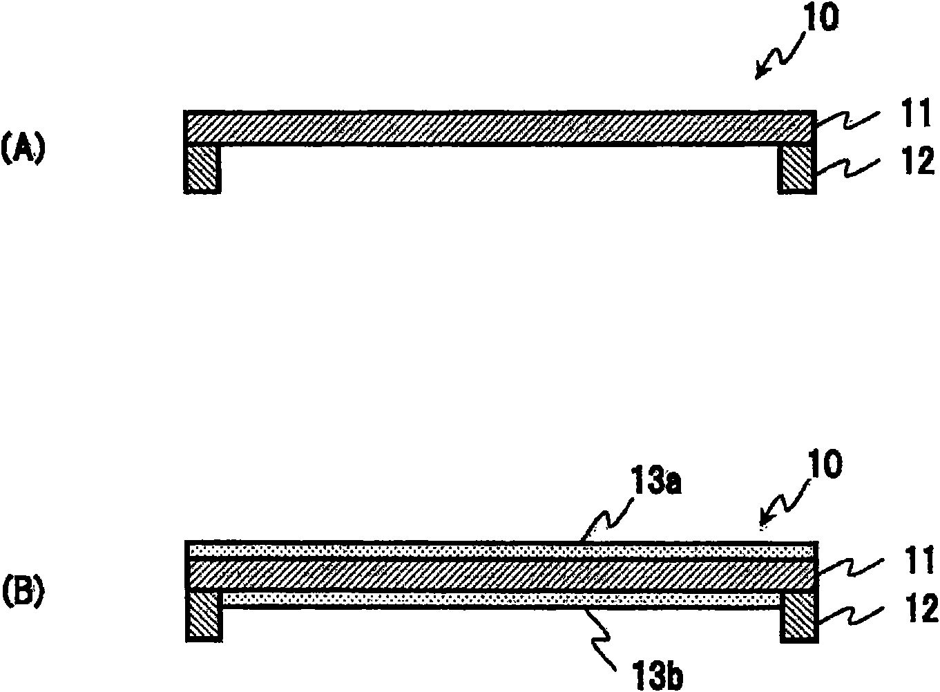
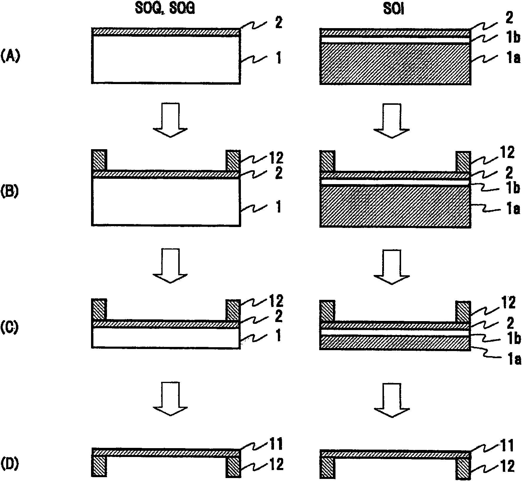
[0057] figure 2 It is an explanatory diagram of the manufacturing process, which is used to illustrate the manufacturing method of the pellicle module of the present invention. SOI substrates in a broad sense include SOQ (Silicon On Quartz) substrates and SOG (Silicon On Glass) substrates, and the support substrate 1 at this time is a quartz substrate and a glass substrate, respectively. Also, the support substrate 1 of an SOI (Silicon On Insulator) substrate in a narrow sense is a substrate on which an oxide film 1b is provided on the surface of a silicon substrate 1a. On the main surfaces of these supporting substrates, a silicon single crystal film 2 having a crystal plane inclined by 3 to 5° from a lattice plane belonging to the {111} plane group as the main surface is provided, and the silicon single crystal film 2 serves as a protective film. . In addition, the silicon single crystal film 2 provided on the supporting substrate has an absorption coefficient of EUV ligh...

Embodiment 2

[0066] according to figure 2In the steps shown, a pellicle assembly in which the pellicle 11 is supported by the pellicle frame 12 is produced, the pellicle 11 is made of a silicon single crystal film, and the silicon single crystal film has a crystallographic orientation for the to direction The azimuth plane with an inclination of 3-5° (3°off to 5°off) is used as the main surface. Also, the thickness of the pellicle film 11 of the silicon single crystal film of this embodiment is 20 nm. Then, on the surface and the bottom surface of the protective film 11 respectively, a SiC thin film with a thickness of several nm is vapor-deposited on the protective film 11 of the silicon single crystal film by gas cluster ion beam evaporation method, so as to coat the protective film. 11.

[0067] For the pellicle modules obtained in Examples 1 and 2, the transmittance of EUV light is above 50%, the processing capacity per unit time during EUV exposure can also reach a practical leve...


PUM

PropertyMeasurementUnit
absorptanceaaaaaaaaaa
visible light transmittanceaaaaaaaaaa

Abstract

A silicon single crystal film having a crystal plane as its principal plane, the crystal plane being inclined at 3 to 5 DEG from any lattice plane belonging to {100} planes or {111} planes is used as a pellicle film (11). The silicon single crystal having such a crystal plane as its principal plane has effective bond density and Young's modulus thereof which are about 40% to about 50% higher than those of a silicon single crystal with orientation, and therefore a cleavage and crack do not easily occur. Moreover, the silicon single crystal has a high chemical resistance such as hydrofluoric acid resistance, and hardly causes an etch pit and void. Accordingly, the present invention can provide a pellicle comprising a pellicle film for EUV having high transmission, and excellent mechanical and chemical stability, as well as having a high yield, and being practical also in cost.

Description

technical field [0001] The present invention relates to a pellicle component for lithography, more specifically, to a pellicle component suitable for extreme ultraviolet (EUV: Extreme Ultra Violet) lithography process and a manufacturing method thereof. Background technique [0002] With the high integration of semiconductor devices, the patterns formed by lithography are also miniaturized, and devices with a pattern width of about 45nm are also entering the practical stage. Such a thin line pattern can be realized by lithography using ArF immersion exposure method or double exposure method, which are improved techniques of conventional excimer exposure technology. [0003] However, lithography based on these excimer exposure techniques is difficult to cope with finer patterns, such as patterns with a width of less than 32nm. Weiying, began to receive attention. [0004] In order to practically use the exposure technology of EUV light with a main wavelength of 13.5nm, it g...

Claims


Application Information

Patent Timeline
Patent Type & Authority Applications(China)
IPC IPC(8): G03F1/14G03F7/20G03F1/22G03F1/24G03F1/62
CPCB82Y10/00G03F1/24G03F1/62B82Y40/00
Inventor 久保田芳宏秋山昌次进藤敏彦
Owner SHIN ETSU CHEM CO LTD
Why Eureka
Try Eureka