

Pattern transferring method
A graphics transfer and graphics technology, which is applied in the direction of electrical components, semiconductor/solid-state device manufacturing, circuits, etc., can solve the problems of poor steepness of the side wall of the photoresist pattern structure, unstable pattern structure, unfavorable etching, etc., to avoid Unstable graphic line structure, avoid uneven and uneven coating, and prevent inconsistent light energy
- Summary
- Abstract
- Description
- Claims
- Application Information
AI Technical Summary
Problems solved by technology
Method used
Image

Examples
Embodiment 1
[0037] This embodiment does not need to coat the anti-reflection layer on the surface of the etched mask layer, so as to avoid the uneven and uneven coating of the anti-reflection layer in the prior art, which will lead to inconsistent light energy received by the photoresist, thereby making the photolithography The graphic line structure formed by the glue layer is unstable and prone to collapse. The specific embodiments of the present invention will be described in detail below in conjunction with the accompanying drawings.
[0038] Such as Figure 6 As shown, the photolithography method of this embodiment includes:
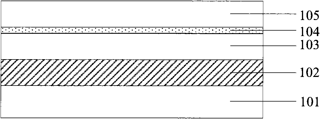
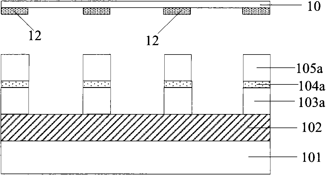
[0039] Step S111, providing a semiconductor substrate that may have two superimposed mask layers, the first mask layer away from the semiconductor substrate is etched to form a patterned first mask layer, and the first patterned mask layer under the patterned first mask layer is exposed. Two mask layers;
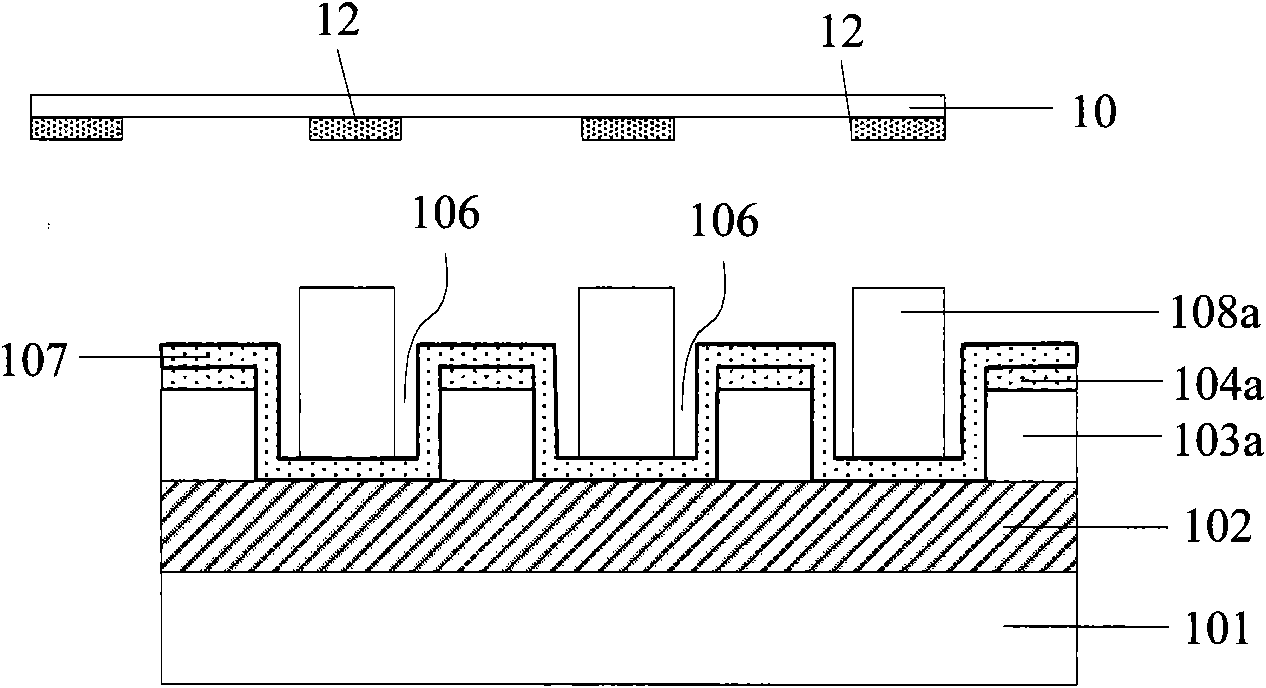
[0040] Step S112, forming a second photoresist layer...
Embodiment 2
[0072] In embodiment 1, after the first mask layer far away from the semiconductor substrate has been etched by conventional methods, when a second photoresist layer having a second semiconductor device pattern is formed on the second mask layer, shallow exposure- The combined method of silylation-plasma etching, but the present invention is not limited thereto, shallow exposure-silylation-plasma can also be used when forming the first photoresist layer with the first semiconductor device pattern on the first mask layer etch joint methods such as Figure 14 As shown, this method includes:
[0073] Step S201, providing a semiconductor substrate with two mask layers, wherein the second mask layer is located between the first mask layer and the semiconductor substrate;
[0074] Step S202, forming a first photoresist layer containing photoacid forming agent and p-alkylphenoxy formic acid resin on the first mask layer;
[0075] Step S203, forming a patterned first photoresist lay...
Embodiment 3
[0085] When there is only one mask layer on the semiconductor substrate, the combined method of shallow layer exposure-silanization-plasma etching can also be used when forming semiconductor device patterns on the mask layer. Such as Figure 15 As shown, this method includes:
[0086] Step S301, providing a semiconductor substrate with a mask layer;
[0087] Step S302, forming a photoresist layer containing photoacid forming agent and p-alkylphenoxy formic acid resin on the mask layer;
[0088] Step S303, forming a patterned photoresist layer by shallow exposure, and the depth of the pattern on the photoresist layer is smaller than the thickness of the first photoresist layer;
[0089] Step S304, performing silanization treatment on the part of the surface of the photoresist layer that is exposed by the shallow layer, and forming a patterned anti-plasma etching layer on the photoresist layer;
[0090] Step S305, using the patterned plasma etching resistant layer on the phot...
PUM
| Property | Measurement | Unit |
|---|---|---|
| strength | aaaaa | aaaaa |
| thickness | aaaaa | aaaaa |
| thickness | aaaaa | aaaaa |
Abstract
Description
Claims
Application Information