Method for preparing evanescent wave coupling type single carrier traveling wave photoelectrical detector

A technology of photodetector and manufacturing method, which is applied in the coupling of optical waveguide, optical waveguide light guide, light guide, etc., and can solve the problems of reducing bandwidth performance and the like

Inactive Publication Date: 2009-12-30
INST OF SEMICONDUCTORS - CHINESE ACAD OF SCI
View PDF0 Cites 12 Cited by
  • Summary
  • Abstract
  • Description
  • Claims
  • Application Information

AI Technical Summary

Problems solved by technology

However, light is slowly coupled into the absorbing layer from the lower dilution waveguide. To obtain a large internal quantum efficiency, a long waveguide length is required to absorb the incident light, but increasing the device size will lead to a large RC time constant, thereby reducing the bandwidth performance.

Method used


Image

  • Method for preparing evanescent wave coupling type single carrier traveling wave photoelectrical detector
  • Method for preparing evanescent wave coupling type single carrier traveling wave photoelectrical detector
  • Method for preparing evanescent wave coupling type single carrier traveling wave photoelectrical detector

Examples


Embodiment Construction

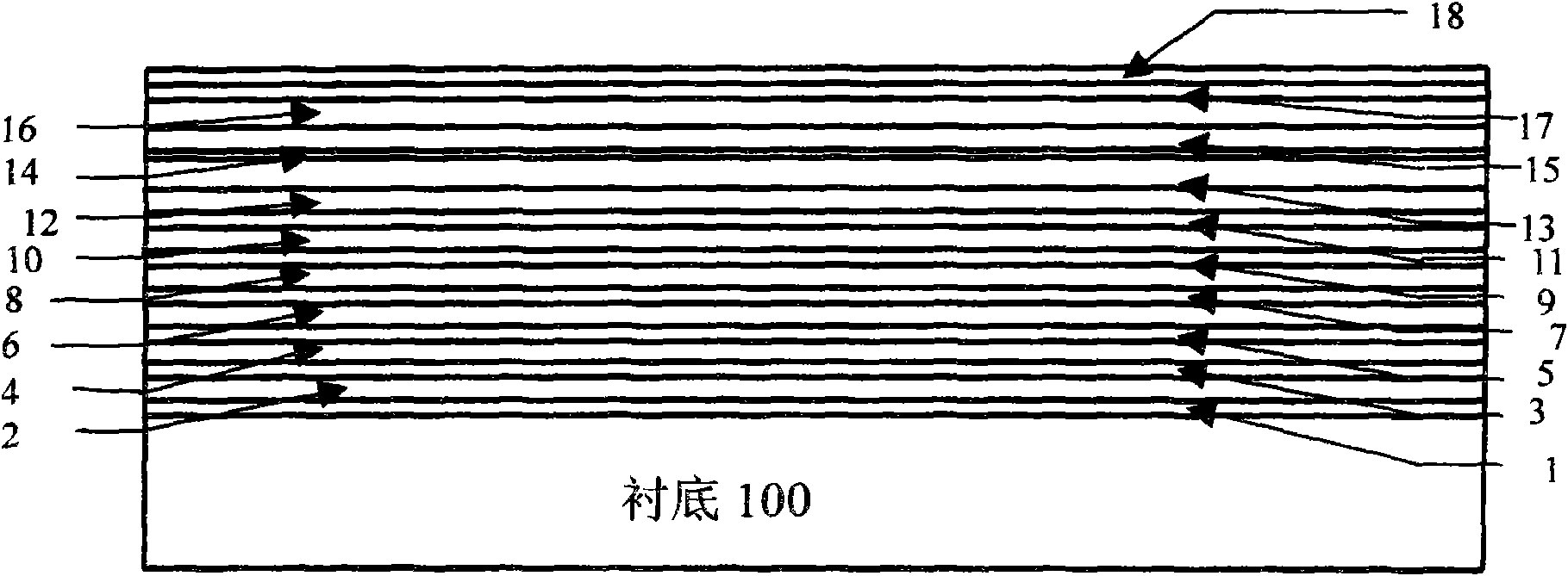
[0027] figure 1 It is a schematic cross-sectional view of one epitaxy on half of the insulating indium phosphide substrate 100 by metal-organic vapor deposition. On the semi-insulating InP substrate 1, a 100nm-thick InP stress buffer layer 1 is first grown on the semi-insulating InP substrate 1 by metal-organic chemical vapor deposition (MOCVD), which is mainly to adjust the lattice mismatch; 5 cycles of 1.2Q quaternary layer / InP layer, 5 cycles of 1.2Q quaternary layer / InP layer are the first 1.2Q quaternary layer 2, the first indium phosphorus layer 3, and the second 1.2Q quaternary layer 4. The second indium phosphorus layer 5, the first n-1.2Q quaternary layer 6, the first n-indium phosphorus layer 7, the second n-1.2Q quaternary layer 8, the second n-indium phosphorus layer 9, the first n-indium phosphorus layer Three n-1.2Q quaternary layers 10, third n-InP layer 11, 1.2Q quaternary layer / InP layer thickness of 5 periods are all 190nm / 110nm, wherein the first 1.2Q quate...


PUM


Abstract

The invention provides a method for preparing an evanescent wave coupling type single carrier traveling wave photoelectrical detector. The method comprises the following steps of: orderly growing layers from an indium-phosphorus stress buffer layer to an InGaAs contact layer on a substrate; growing a layer of silicon oxide masking film on the InGaAs contact layer; etching both sides of the silicon oxide masking film, etching both sides of a silicon oxide masking strip, and obtaining a deep ridge structure; corroding partial deep ridge structure by a wet method, and forming an incident window region; forming N-shaped metal ohmic contacts on both sides of the deep ridge structure by a lift-off method; etching all layers outside the outer side edge of the N-shaped metal ohmic contact on the substrate; keeping all layers on the side of the incident window region, and forming a mesa structure on the substrate; preparing a signal electrodes of the titanium traveling wave electrode structure on the part extended from the upper surface of the deep ridge structure to the substrate by an inclined mesa; preparing a grounding electrode of the titanium traveling wave electrode structure on the part extended from the N-shaped metal ohmic contact on both sides of the deep ridge structure to the substrate by the inclined mesa; and reducing and splitting.

Description

technical field [0001] The invention belongs to the technical field of semiconductors, and relates to a manufacturing method of an evanescent wave coupled photodetector with a traveling wave electrode structure, in particular to a manufacturing method of a traveling wave electrode single carrier detector and an evanescent waveguide integrated device. Background technique [0002] Modern high-performance optical communication, signal processing and measurement systems require photodetectors to have high response speed and high saturation output, and long-wavelength photodetectors of III-V compound semiconductors have also become the focus of research. [0003] Wide bandwidth, high responsivity, and high output saturation power detectors have two mainstream development directions. One is edge-coupled PD, which has consistent scattered and consistent photocurrent, such as velocity matching distribution detectors and decoupling detectors. One is to reduce the space charge effect...

Claims


Application Information

Patent Timeline
Patent Type & Authority Applications(China)
IPC IPC(8): G02B6/136G02B6/13G02B6/42
Inventor 张云霄廖栽宜赵玲娟朱洪亮潘教青王圩
Owner INST OF SEMICONDUCTORS - CHINESE ACAD OF SCI
Why Eureka
Try Eureka