Method for preparing transparent thin-film transistor of alloyed oxide

A thin film transistor and transparent thin film technology, which is applied in the field of semiconductor single crystal thin film preparation, can solve the problems of insufficient flexibility of ZnO thin film, high carrier concentration and high annealing temperature, so as to improve field effect mobility, high mobility, The effect of low manufacturing temperature

Inactive Publication Date: 2009-12-30
ZHEJIANG UNIV
View PDF1 Cites 13 Cited by
  • Summary
  • Abstract
  • Description
  • Claims
  • Application Information

AI Technical Summary

Problems solved by technology

In 2003, Nomura et al. used single crystal InGaO3(ZnO) 5 A mobility of 80cm was obtained 2 /V·s, switch ratio 10 6 TFT devices, but the annealing temperature of this technology is very high
[0006] In the existing thin-film transistor (TFT) patent (application number 03811678.2), there are the following points to be improved: (1) high temperature process (300-1000°C) is required, and this technology is used in actual LCD and OLED flat panel displays

Method used


Image

  • Method for preparing transparent thin-film transistor of alloyed oxide
  • Method for preparing transparent thin-film transistor of alloyed oxide
  • Method for preparing transparent thin-film transistor of alloyed oxide

Examples


Embodiment Construction

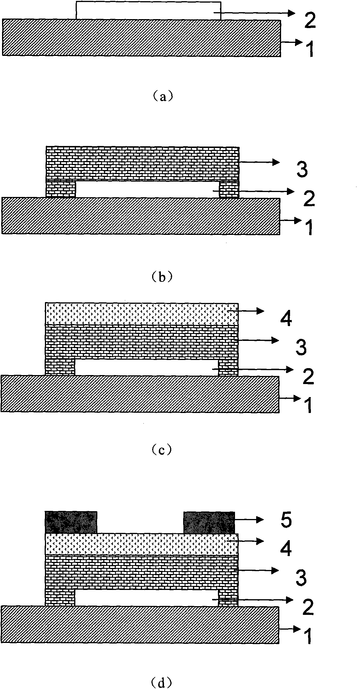
[0058] Below through specific embodiment, further illustrate substantive characteristic and remarkable progress of the present invention.

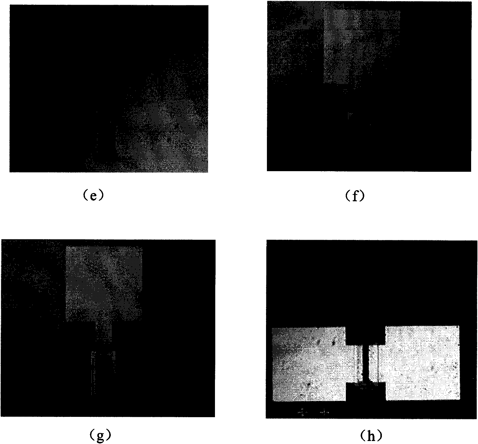
[0059] (1) photoetching ITO gate electrode 2, see figure 1 (a) and see figure 2 (e)

[0060] 1) Cleaning ITO glass 1, carbon tetrachloride, acetone, and alcohol ultrasonic cleaning three times, each for three minutes. Then rinse repeatedly with deionized water.

[0061] 2) Drying: Put the cleaned ITO glass into an oven and dry at 120°C for 30 minutes;

[0062] 3) Coating: Spray the photoresist on the ITO surface with a coating machine, the rotation speed of the coating machine is 6000 rpm, the coating is 40s, and the thickness of the coating is 1.1 μm;

[0063] 4) Pre-baking: put the ITO glass with the photoresist on it in an oven, and bake it at 80°C for 20 minutes;

[0064] 5) Exposure: UV exposure for 40s;

[0065] 6) Developing: a developer solution with a ratio of 1:1 (deionized water), the developing time is about 22s (the tim...


PUM

PropertyMeasurementUnit
Thicknessaaaaaaaaaa
Thicknessaaaaaaaaaa
Thicknessaaaaaaaaaa

Abstract

The invention relates to a method for preparing a transparent thin-film transistor at low temperature. A small amount of In2O3 and SnO2 are mixed in ZnO to form a transparent ZnInSnO quaternary alloy semiconductor thin film to be a channel layer, the method is compatible with the technology for preparing flat displays and the like at low temperature, the transparent thin-film transistor is prepared by magnetron sputtering low-temperature growth, and the technology of the combinations of bottom-gate structure and lithography, chemical wet etching and stripping is adopted. Compared with the existing silicon-based TFT technology, oxide TFT has the characteristics of transparent visible light, high migration rate, low preparing temperature and the like. The transparent thin-film transistor can be applied to active-matrix liquid crystal display devices, printers, copiers and cameras and the like.

Description

technical field [0001] The invention belongs to the technical field of preparation of semiconductor single crystal thin films, in particular to a method for manufacturing oxide thin film transistors at low temperature Background technique [0002] Thin-film transistors, invented in the 1960s, have now been widely used, with fast development and wide application fields. From low-temperature amorphous silicon TFT to high-temperature polysilicon TFT, the technology is becoming more and more mature, and the application object has also developed from only driving LCD (liquid Crystal Display) to driving both LCD and OLED (Organic Light Emitting Display), and even electronic paper. With the continuous improvement of the semiconductor process level, the pixel size is continuously reduced, and the resolution of the display screen is also getting higher and higher. [0003] The 21st century is the era of flat panel display in the field of display, and the vast majority of flat panel ...

Claims


Application Information

Patent Timeline
IPC IPC(8): H01L21/336
Inventor 吴惠桢朱夏明原子健张莹莹王雄
Owner ZHEJIANG UNIV
Why Eureka
Try Eureka