Printable semiconductor structures and related methods of making and assembling

A semiconductor and structural technology, applied in the fields of printable semiconductor structures and related manufacturing and assembly, which can solve the problems of destruction, cracking, damage, etc.

Active Publication Date: 2010-01-20
THE BOARD OF TRUSTEES OF THE UNIV OF ILLINOIS
View PDF1 Cites 33 Cited by
  • Summary
  • Abstract
  • Description
  • Claims
  • Application Information

AI Technical Summary

Problems solved by technology

Second, although many amorphous silicon, organic or hybrid organic-inorganic semiconductors can be compatible incorporated into plastic substrates and can be processed at relatively low temperatures, these materials do not have the integration capabilities that would provide good electronic properties. Electronic Characteristics of Electronic Devices
This mechanical stress can lead to damage to individual components, such as cracking, and can also degrade or break electrical contacts between device components

Method used


Image

  • Printable semiconductor structures and related methods of making and assembling
  • Printable semiconductor structures and related methods of making and assembling
  • Printable semiconductor structures and related methods of making and assembling

Examples


Embodiment 2

[0119] Example 2: Gigahertz operation of a mechanically flexible transistor on a flexible plastic substrate

[0120] The combined use of GaAs wires with ohmic contacts formed from bulk wafers, soft lithographic transfer printing techniques, and optimized device designs enables the formation of mechanically flexible transistors on low-cost plastic substrates with individual device speeds in the gigahertz range and with High mechanical bendability. The methods disclosed herein include materials that are fabricated with limited lithographic image forming resolution and registration in a simple layout. This example describes the electrical and mechanical properties of high performance transistors. These results are of great importance in certain applications including, but not limited to, high-speed communications and computing, and emerging types of large-area electronic systems ("macroelectronic devices").

[0121] Large-area flexible electronic systems (ie, macroelectronic de...

Embodiment 3

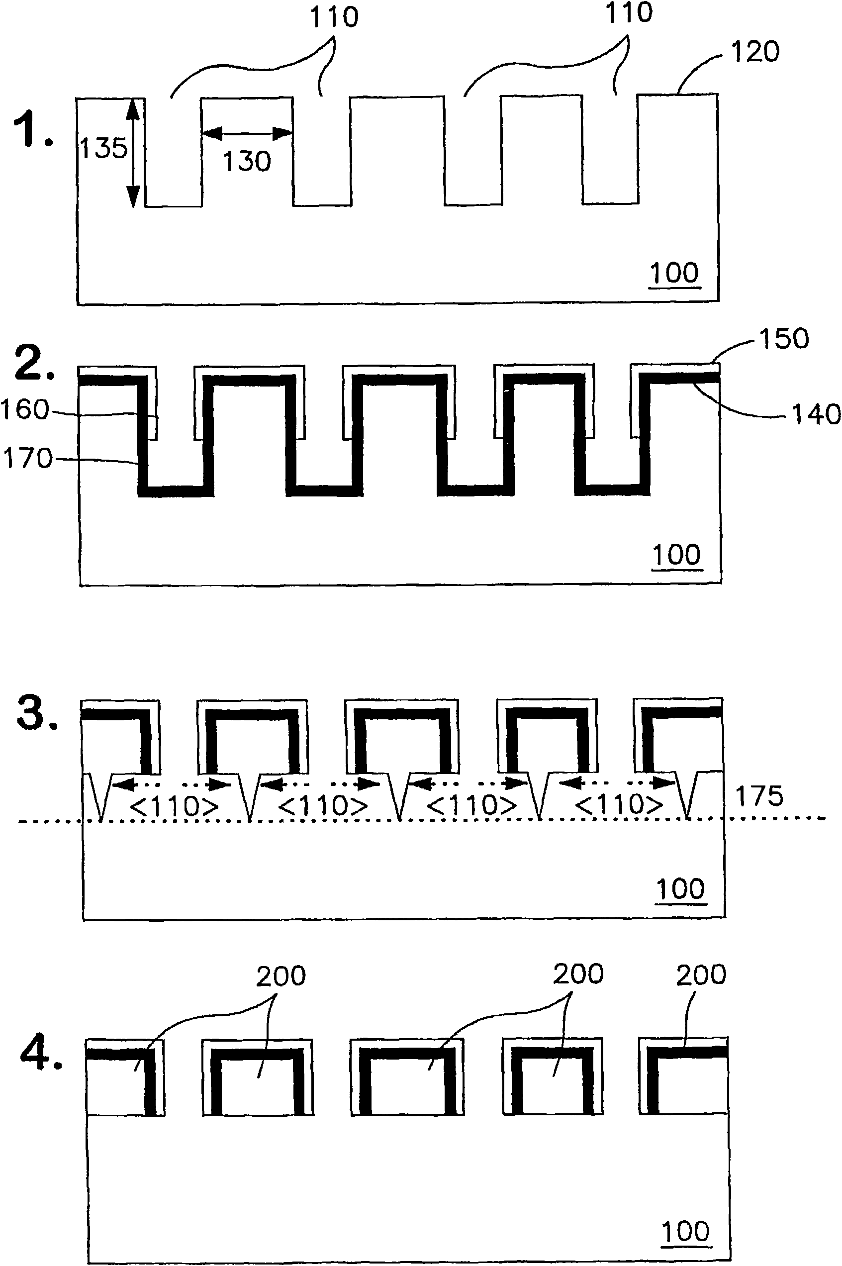
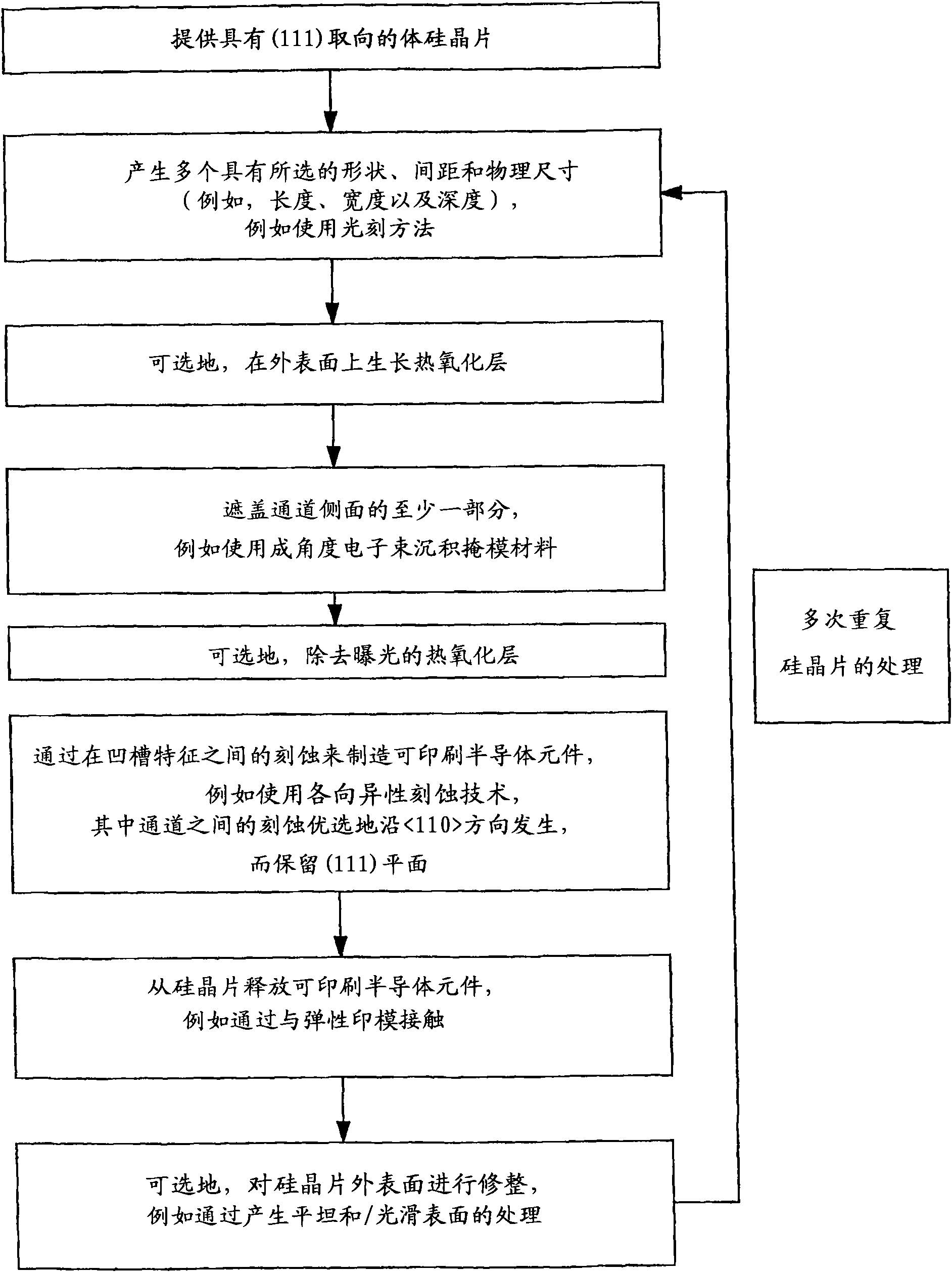
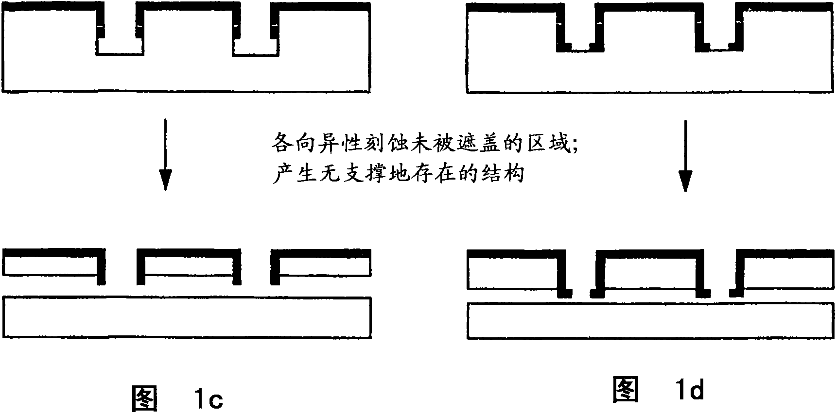
[0144] Example 3 Mechanically Flexible Thin Film Transistors Using Ultra-Thin Silicon Ribbons Harvested from Bulk Wafers

[0145] This example describes a thin-film transistor using an aligned array of thin (sub-micron) ribbons of single-crystal silicon that is patterned by lithography and bulk silicon ( 111) produced by anisotropic etching of the wafer. Devices incorporating such ribbons printed onto thin plastic substrates showed good electrical properties as well as mechanical flexibility. Effective device mobility, as estimated in the linear region, up to 360cm 2 V -1 the s -1 and on / off ratio > 10 3 . These results represent an important advance in low-cost methods for fabricating large-area, high-performance, mechanically flexible electronic systems for structural health monitoring, sensors, displays, and other applications.

[0146]Confinement-related properties and wide-ranging form factors make low-dimensional materials promising new applications in electronics,...

Embodiment 4

[0151] Example 4 Bendable GaN High Electron Mobility Transistor (HEMT) on Plastic Substrate

[0152] The emerging field of macro-electronic devices encompasses flexible large-area electronics, technology that has witnessed considerable progress over the past few years, and has several major users as well as military applications. In the near future, They are expected to be commercialized. Microelectronic circuits with novel form factors are key components of these systems, and new fabrication methods, especially printing methods, will likely be required to manufacture them. For this reason, considerable attention has been devoted to printable forms of semiconductors, and both organic (eg benzene, polythiourea, etc.) and inorganic (eg polysilicon, inorganic nanowires) materials have been investigated. The work has shown some promising results for devices integrated on plastic substrates. However, the applied current range is limited by the inherent poor performance of devices...


PUM


Abstract

The present invention provides a high yield pathway for the fabrication, transfer and assembly of high quality printable semiconductor elements having selected physical dimensions, shapes, compositions and spatial orientations. The compositions and methods of the present invention provide high precision registered transfer and integration of arrays of microsized and / or nanosized semiconductor structures onto substrates, including large area substrates and / or flexible substrates. In addition, the present invention provides methods of making printable semiconductor elements from low cost bulk materials, such as bulk silicon wafers, and smart-materials processing strategies that enable a versatile and commercially attractive printing-based fabrication platform for making a broad range of functional semiconductor devices.

Description

[0001] Cross-references to related applications [0002] This application claims U.S. Patent Application No. 11 / 145,542, filed June 2, 2005, U.S. Patent Application No. 11 / 145,574, filed June 2, 2005, and International PCT Application No. .PCT / US05 / 19354 priority, hereby incorporated by reference, to the extent not inconsistent with the disclosure herein, the contents of all of these applications. Background technique [0003] Since the first demonstration of printed all-polymer transistors in 1994, potential new types of electronic systems that include flexible integrated electronics on plastic substrates have attracted considerable attention. [Gamier, F., Hajlaoui, R., Yassar, A. and Srivastava, P., Science, Vol. 265, pp. 1684-1686]. More recently, fundamental research has focused on developing new solution-processable materials for semiconductors, insulators, and semiconductor components for use in flexible plastic electronics. However, progress in the field of flexible e...

Claims


Application Information

Patent Timeline
Patent Type & Authority Applications(China)
IPC IPC(8): H01L21/302H01L21/8242H01L23/62H05K3/36H01R12/00H01L21/77
CPCH01L2924/0002
Inventor R·G·纳佐J·A·罗杰斯E·梅纳德李建宰姜达荣孙玉刚M·梅尔特朱正涛高興助S·麦克
Owner THE BOARD OF TRUSTEES OF THE UNIV OF ILLINOIS
Why Eureka
Try Eureka