Single-mode high-power vertical cavity surface emitting laser and manufacturing method thereof

A technology of vertical cavity surface emission and manufacturing method, which is applied in the field of structure and production of vertical cavity surface emitting lasers, can solve the problem of low output power of photonic crystal VCSEL, achieve improved thermal characteristics, increase oxidation aperture, and increase single-mode output The effect of power

Active Publication Date: 2010-03-10
INST OF SEMICONDUCTORS - CHINESE ACAD OF SCI
View PDF0 Cites 44 Cited by
  • Summary
  • Abstract
  • Description
  • Claims
  • Application Information

AI Technical Summary

Problems solved by technology

[0010] However, so far, the output power of the existing photonic crystal VCSEL is not hi

Method used


Image

  • Single-mode high-power vertical cavity surface emitting laser and manufacturing method thereof
  • Single-mode high-power vertical cavity surface emitting laser and manufacturing method thereof
  • Single-mode high-power vertical cavity surface emitting laser and manufacturing method thereof

Examples


Embodiment 1

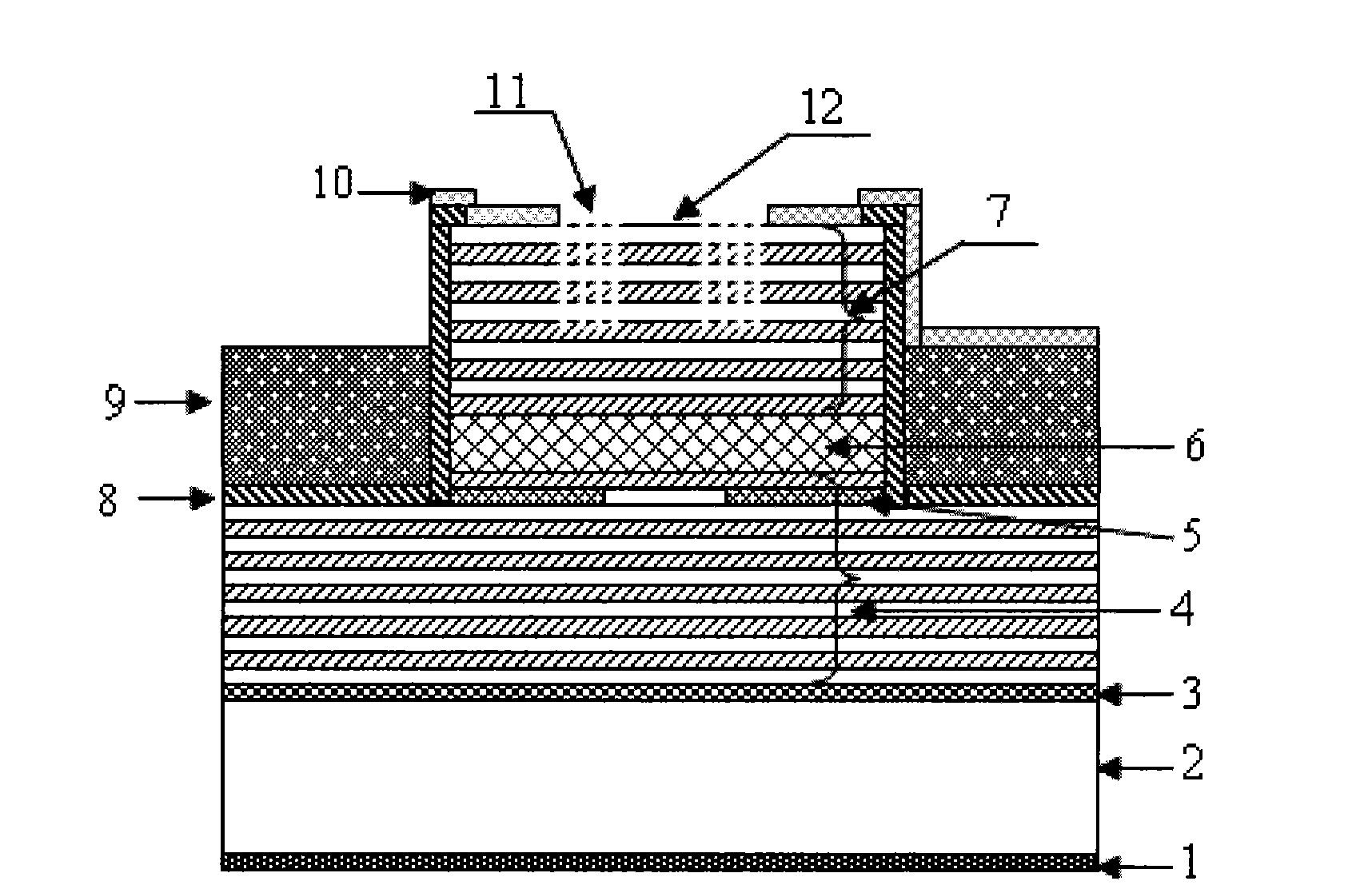
[0034] Embodiment 1: P-type electrode 1 is TiAu, P-type electrode 1 is made on the back side of Si substrate 2, P-type Si substrate 2, metal bond layer 3 is TiAu / Sn / AuTi, by metal bond layer 3 Si substrate 2 and P-type distributed Bragg reflector (DBR) 4 are bonded together, P-type distributed Bragg reflector (DBR) 4, 28 periodic modulation doping and composition gradient Ga0.1Al0.9As / Al0. Alternate composition of 9Ga0.1As material, connected with the active region 6 that can provide gain, used to provide high reflectivity, and at the same time form a current injection channel, P-type DBR4 contains a layer of high aluminum composition near the active region The oxidation confinement layer 5 is used to form electro-optic confinement. The active region 6 is sandwiched between P-type DBR4 and N-type DBR7 to provide optical gain. The active region 6 is composed of three AlInGaAs quantum wells, and the thickness of the active region is is 1λ, λ is the lasing wavelength, N-type DBR7...

Embodiment 2

[0048] Embodiment 2: single-mode high-power VCSEL with a wavelength of 980nm, the middle multi-quantum well active region 7 is made of InGaAs / GaAs material, and the N-type DBR7 and P-type DBR4 are respectively modulated and doped with gradually changing composition GaAs / Al 0.9 Ga 0.1 As, other components are the same as in Embodiment 1.

Embodiment 3

[0049] Embodiment 3: a single-mode high-power VCSEL with a wavelength of 1310nm, the middle multi-quantum well active region 6, adopts GaInNAs / GaAs, or quantum dot materials, N-type DBR7 and P-type DBR4 respectively adopt modulation doping and composition gradient GaAs / Al 0.9 Ga 0.1 As material, other parts are the same as in Example 1.


PUM

PropertyMeasurementUnit
Thicknessaaaaaaaaaa

Abstract

The invention relates to a single-mode high-power vertical cavity surface emitting laser (VCSEL), which belongs to the field of semiconductor photoelectronics. The laser is characterized by comprisinga P-type electrode (1), a P-type Si substrate (2), a metal bonding layer (3), a P-type distributed Bragg reflector (DBR) (4), an oxide limiting layer (5), an active area (6), an N-type DBR (7), a SiO2 mask (8), polymide or benzocyclobutene (BCB) (9), an N electrode (10), a photonic crystal (11) and a light-exiting window (12). The introduction of the photonic crystal into the vertical cavity surface emitting laser with the structure can enlarge an oxidation aperture and improve the single-mode output power; and at the same time, the transfer of the conventional VCSEL epitaxial wafer to the Sisubstrate by adopting bonding technology and the adoption of a design of exiting light at the bottom are convenient for narrowing the distance between a VCSEL epitaxial wafer active area and the Si substrate, improving the thermal characteristics of devices and further improving the single-mode output power.

Description

technical field [0001] The invention relates to the technical field of vertical-cavity surface-emitting lasers, in particular to the structure and manufacturing method of a single-mode high-power vertical-cavity surface-emitting laser. Background technique [0002] Vertical cavity surface emitting laser (VCSEL) has good monochromaticity, small divergence angle, single longitudinal mode lasing, low threshold current, high modulation bandwidth, easy coupling with fiber, easy high-density integration, "on-chip" detection and low cost And other advantages, widely used in laser printing, optical storage, density optical storage and readout, free space optical interconnection and high-speed data transmission in single-mode optical fiber, etc. However, in these practical applications, VCSELs are often required to operate in a stable fundamental transverse mode, especially in a fundamental transverse mode with high output power. The traditional method of preparing single-mode VCSEL...

Claims


Application Information

Patent Timeline
IPC IPC(8): H01S5/183H01S5/187H01S5/343
Inventor 渠红伟郑婉华刘安金王科张冶金彭红玲陈良惠
Owner INST OF SEMICONDUCTORS - CHINESE ACAD OF SCI
Why Eureka
Try Eureka