Resistance random memory based on columbium oxide film and preparation method thereof

A technology of random access memory and niobium oxide, which is applied in the field of memory, can solve the problems of guaranteeing the characteristics of stoichiometric devices, etc., and achieve the effects of large application value, long data retention time, excellent transition and memory characteristics

Inactive Publication Date: 2010-03-17
FUDAN UNIV
View PDF0 Cites 8 Cited by
  • Summary
  • Abstract
  • Description
  • Claims
  • Application Information

AI Technical Summary

Problems solved by technology

However, most of the current research uses physical vapor deposition or thermal oxidation to prepare samples. These preparation methods are difficult to guarantee device characteristics in terms of stoichiometry, ultra-thin thickness control, and step coverage.

Method used


Image

  • Resistance random memory based on columbium oxide film and preparation method thereof
  • Resistance random memory based on columbium oxide film and preparation method thereof
  • Resistance random memory based on columbium oxide film and preparation method thereof

Examples


Embodiment

[0023] Below in conjunction with accompanying drawing and specific embodiment the present invention is described in further detail:

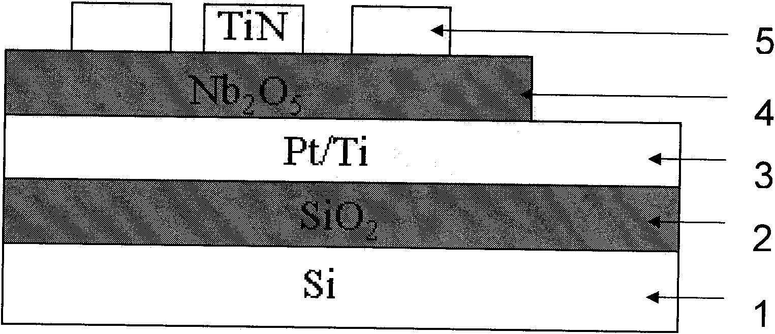
[0024] A silicon dioxide dielectric layer 1 is grown on a single crystal silicon 2 by means of thermal oxidation or chemical vapor deposition as a substrate. The oxidation temperature is 1100°C, the oxidation time is 5 minutes, and the thickness of the silicon dioxide layer is 150nm-200nm. Pt / Ti (80nm / 20nm) was prepared as the bottom electrode layer 3 by sputtering growth method. The sample was placed in the atomic layer deposition apparatus, and the wafer was heated to about 300°C before the first pulse in the pulse cycle. This temperature was maintained throughout the ALD growth period. The reaction chamber was brought to a pressure of about 1 Torr prior to the first pulse in the pulse cycle and maintained at this pressure throughout the process.

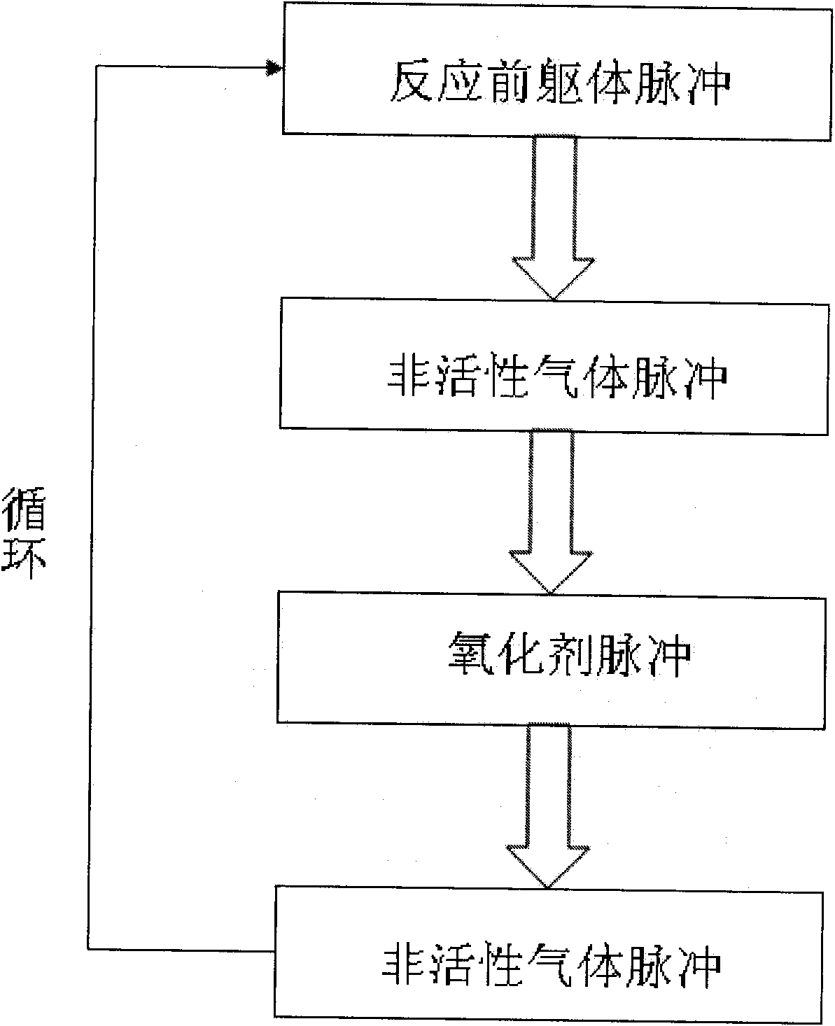
[0025] The pulse period is figure 2 shown in . The pulse cycle includes the following step...


PUM

PropertyMeasurementUnit
thicknessaaaaaaaaaa
thicknessaaaaaaaaaa
thicknessaaaaaaaaaa

Abstract

The invention relates to a resistance random memory based on a columbium oxide film and a preparation method thereof, belonging to the technical field of memories. The memory unit comprises a substrate and a metal-insulation layer-metal (MIM) structure unit, wherein a top electrode of the MIM structure unit is metal films, such as titanium nitride and the like, the insulation layer is a columbiumoxide film, and a lower electrode adopts Pt or Au. The MIM structure in the invention represents excellent transformation and memory properties between high and low resistance states under the continuous scanning excitation of direct-current voltage. Further, the invention also provides the preparation method of the memory unit. The method comprises the preparation of a substrate material, the lower electrode, a dielectric film and an upper electrode and the like.

Description

technical field [0001] The invention belongs to the technical field of memory, and in particular relates to a resistance random access memory with resistance transition and memory characteristics and a preparation method thereof. Background technique [0002] With the further shrinking of the feature size of semiconductor devices, the traditional FLASH memory is limited by its own conditions and cannot meet the needs of the rapid development of integrated circuit technology. The development of next-generation non-volatile memories has recently aroused intense interest in the industry. Ferroelectric memory (FRAM), magnetoresistive memory (MRAM), and phase change memory (PRAM) have received attention one after another. In recent years, research on a resistive random access memory (RRAM) technology based on material resistance changes has become the focus of attention. The basic memory cell of RRAM consists of a metal-insulator-metal (MIM) structured resistor. By means of vo...

Claims


Application Information

Patent Timeline
Patent Type & Authority Applications(China)
IPC IPC(8): H01L45/00G11C11/56
Inventor 陈琳孙清清王鹏飞丁士进张卫
Owner FUDAN UNIV
Why Eureka
Try Eureka