Method for processing silicon base material, article processed by the method, and processing apparatus

A processing method and processing device technology, applied in the field of processed products and processing devices of crystalline silicon substrates, can solve the problem of high manufacturing cost

Inactive Publication Date: 2010-03-24
QUANTUM 14
View PDF2 Cites 14 Cited by
  • Summary
  • Abstract
  • Description
  • Claims
  • Application Information

AI Technical Summary

Problems solved by technology

However, in previous cases, using such as Figure 23 As shown in B, the processing method of gradually forming the micro-holes 14 through the surface and the back of the substrate with laser 33 has the disadvantage of high manufacturing cost.

Method used


Image

  • Method for processing silicon base material, article processed by the method, and processing apparatus
  • Method for processing silicon base material, article processed by the method, and processing apparatus
  • Method for processing silicon base material, article processed by the method, and processing apparatus

Examples


Embodiment 1

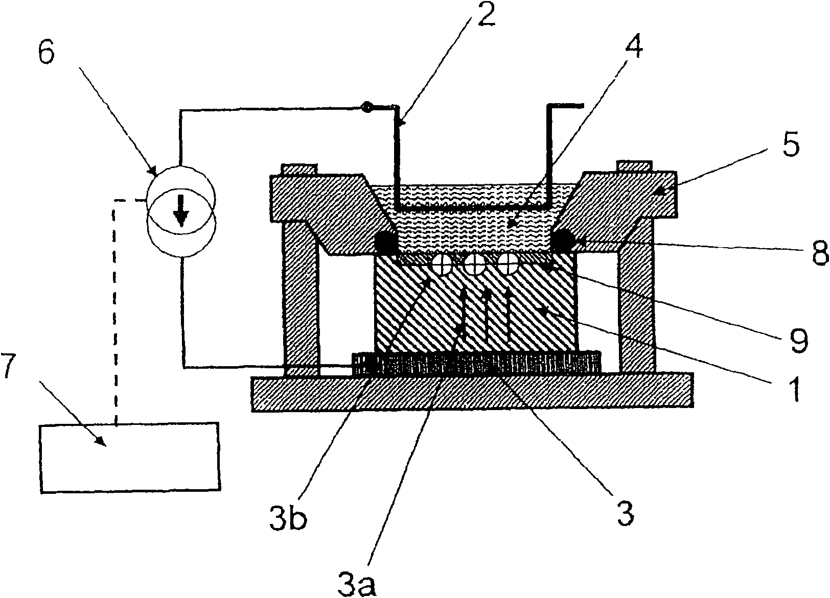
[0073] Figure 9 It is a cross-sectional view of an example of the present invention, showing the progress of anodic oxidation when micropores are formed on a silicon substrate in the order of A and B. use Figure 9 A shows the configuration of the device. 1 is a workpiece, which is a p-type silicon substrate having a resistivity of 1 Ω·cm, a thickness of 200 μm, and a square of 100 mm. The silicon substrate 1 is fixed to an electrolytic cell composed of a metal fixing jig and anode 3 and a support frame made of Teflon (registered trademark) through an organic conductive solid electrode (trade name: Nafion film) 3c with a thickness of about 200 μm. 5 on. A 1:1 mixed electrolyte solution 4 of 49% hydrofluoric acid aqueous solution and ethanol is held by the silicon substrate 1 and the electrolytic cell 5 . An O-ring seal 8 was provided on a portion of the lower surface of the support frame made of Teflon (registered trademark) that was in contact with the silicon substrate ...

Embodiment 2

[0084] Using Figure 10 In the processing of the silicon substrate in the configuration in which the electrolytic solution is supplied to the tip of the cathode described above, it has been demonstrated that the silicon substrate can be etched faithfully according to the shape of the cathode. If this property is utilized, the projected shape of the cathode can be arbitrarily shaped in advance, and the surface of the silicon substrate can be dug in an arbitrary shape. Figure 12 is an example of Figure 12 A is the plan view of the cathode, Figure 12 B is Figure 12 Elevation of section X-X' of A.

[0085] Figure 12 Among them, 2 is a protrusion processed into a height of about 5 mm and a cross-shaped projected shape on a plan view, and is installed on the base 2e. The material of the submount 2 e may be a metal other than platinum, but it is desirable that the surface thereof be covered with the insulating coating film 17 . In addition, the protruding portion 2 may be ...

Embodiment 3

[0088] elephant Figure 7 As already described, silicon ingot slicing can be performed by using the present invention. use Figure 13 Describe its implementation status. Figure 13 19 is the main drive roller, two 19a are the guide rollers of the wire, and 19b and 19c are respectively the sending and recovery bobbins of the wire. The platinum wire 2 is conveyed from the wire sending bobbin 19b, wound around the guide roller 19a and the main roller 19 several times, and then collected on the recovery bobbin 19c. A silicon ingot 1 is mounted on a waterproof anode 3 provided on the bottom of an electrolytic tank 5, and the electrolytic tank 5 is filled with an electrolytic solution 4 to such an extent that the silicon ingot is soaked. The main roller 19 is electrically connected to the cathode side of the power supply 6 , and the anode side of the power supply 6 is electrically connected to the bottom of the silicon ingot 1 through the waterproof anode 3 at the bottom of the e...


PUM

PropertyMeasurementUnit
diameteraaaaaaaaaa

Abstract

In a state where a silicon base material (1) is used as an anode, a fine platinum member (2) is used as a cathode, and an electrolyte solution (4) is arranged between the anode and the cathode, anodicoxidation is performed in constant current mode under the conditions where porous formation mode and electrolytic polishing mode coexist. The platinum member (2) is fitted in the silicon base material (1) with silicon elution, and processes such as hole making, cutting, single-side pressing are performed. Since the silicon base material can be processed at a room temperature with small energy, the crystal quality of the processing surface is not deteriorated. Thus, efficient and highly accurate processing can be performed without using a mechanical method, which consumes much material in conventional processes such as cutting of solar cell silicon base material, and without using laser whose energy unit cost is high, and furthermore, without leaving a crystal damage on a processed surface.

Description

technical field [0001] The present invention relates to a method for processing a silicon substrate, its processed product and a processing device. More specifically, the present invention relates to a method for processing a crystalline silicon substrate useful in the manufacture of precision processed products, transistors, LSIs, solar cells, etc., and a processed product of a crystalline silicon substrate processed by the method, and also uses Its parts and elements, and the processing equipment used to carry out the processing. Background technique [0002] Among the solar cells provided at the time of solar power generation, crystalline silicon solar cells are the most manufactured and used. However, the current situation is that compared with conventional power generation methods such as thermal power, hydraulic power, and atomic energy, the cost of electricity generated by solar power generation is still high. Therefore, in order to widely spread this renewable energ...

Claims


Application Information

Patent Timeline
Patent Type & Authority Applications(China)
IPC IPC(8): C25F3/12B23H3/06B23H3/08C25D11/32
CPCH01L31/1804C25F3/12C25D5/04B23H3/08C25D11/32B23H3/06C25D17/00Y02E10/50C25D17/10C25F3/14C25D17/12Y02E10/547C25D5/022C25D17/001Y02P70/50H02S99/00H01L31/04
Inventor 蕨迫光纪岛田寿一越田信义伯尔拿德·杰路知兼堀惠一
Owner QUANTUM 14
Why Eureka
Try Eureka