Method for eliminating intrinsic electric field in ZnSe/BeTe II quantum well
A quantum well, molecular beam technology, applied in nanotechnology, nanotechnology, nanostructure manufacturing, etc., can solve problems such as the application of optoelectronic devices for observation of unfavorable high-density phenomena
- Summary
- Abstract
- Description
- Claims
- Application Information
AI Technical Summary
Problems solved by technology
Method used
Image

Examples
Embodiment 1
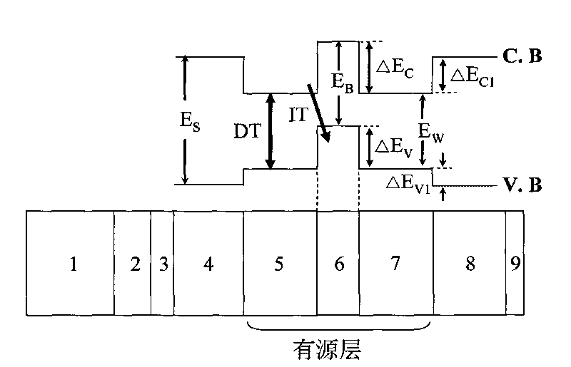
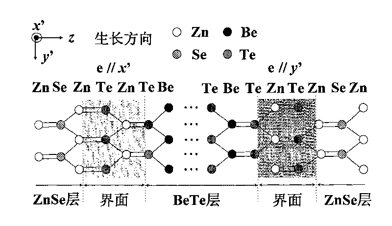
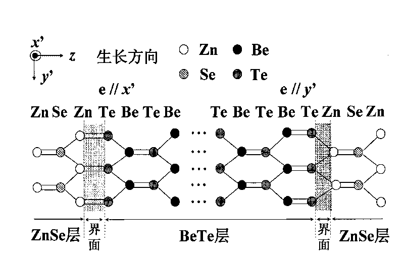
[0038] A method for preparing a ZnSe / BeTe / ZnSe II quantum well with a special interface structure by a molecular beam epitaxy (MBE) growth method, such as Figure 1-2 As shown, the steps are as follows:
[0039] 1. Fix the (001) oriented gallium arsenide substrate on the molybdenum (Mo) sample holder with indium (In);
[0040] 2. Cool the growth chamber with liquid nitrogen, and confirm that the vacuum degree of the III-V growth chamber is 1×10 -10 After the Torr is below, the sample is transferred to the III-V growth chamber through the magnetic transfer rod; the sample holder, the K-cell container with the As solid source and the K-cell container with the Ga solid source are heated to reach The set temperatures are 300°C, 100°C and 750°C respectively;
[0041] 3. Adjust the temperature of the As source K-cell container from 100°C to 295°C, then set the temperature of the sample holder and the Ga source K-cell container to 550°C and 915°C respectively, and start to heat up ...
Embodiment 2
[0055] Embodiment 2 of the present invention is the same as Embodiment 1, except:
[0056] The growth time of the gallium arsenide buffer layer in step 5 is 38 minutes, and the growth thickness is about 320nm;
[0057] The substrate in step 9 is heated up to 330°C;
[0058] When the growth thickness of the isolation layer in step 11 is 300nm, the growth is terminated, and the Se, Be, and Mg sources are first turned off, and then the Zn source is turned off after about 7 seconds;
[0059] When the thickness of the ZnSe layer grown in step 12 is about 20ML, the growth is over, first turn off the Se source, and then turn off the Zn source after about 7 seconds, so as to form a Zn-rich surface layer;
[0060] Before the BeTe layer grows in step 13, turn on the Zn source first, turn off the Zn source after about 7 seconds, and turn on the Te source at the same time, and turn off the Te source after about 7 seconds. The above-mentioned operation of the Zn source and the Te source ...
Embodiment 3
[0064] Embodiment 3 of the present invention is the same as Embodiment 1, except:
[0065] The growth time of the gallium arsenide buffer layer in step 5 is 43 minutes, and the growth thickness is about 360nm;
[0066] The substrate in step 9 is heated up to 340°C;
[0067] When the growth thickness of the isolation layer in step 11 is 330nm, the growth is terminated, and the Se, Be, and Mg sources are first turned off, and then the Zn source is turned off after about 9 seconds;
[0068] When the thickness of the ZnSe layer grown in step 12 is about 28ML, the growth ends, first turn off the Se source, and then turn off the Zn source after about 9 seconds, so as to form a Zn-rich surface layer;
[0069] Before the growth of the BeTe layer in step 13, first turn on the Zn source, turn off the Zn source after about 9 seconds, and turn on the Te source at the same time, and turn off the Te source after about 9 seconds. The above operations of the Zn source and the Te source were...
PUM
 Abstract
Description
Claims
Application Information
 - R&D
- Intellectual Property
- Life Sciences
- Materials
- Tech Scout
- Unparalleled Data Quality
- Higher Quality Content
- 60% Fewer Hallucinations
Browse by: Latest US Patents, China's latest patents, Technical Efficacy Thesaurus, Application Domain, Technology Topic, Popular Technical Reports.
© 2025 PatSnap. All rights reserved.Legal|Privacy policy|Modern Slavery Act Transparency Statement|Sitemap|About US| Contact US: help@patsnap.com