Method for preparing binary alternatively-doped BST membrane

A technology of alternate doping and thin film, which is applied in nanostructure manufacturing, nanotechnology, nanotechnology, etc., can solve the problems of large difference in composition between thin film and target material, expensive equipment, and slow deposition rate of radio frequency magnetron sputtering, etc., to achieve improvement Interface matching relationship, the effect of improving the comprehensive dielectric tuning performance

Inactive Publication Date: 2010-06-02
UNIV OF ELECTRONICS SCI & TECH OF CHINA
View PDF0 Cites 9 Cited by
  • Summary
  • Abstract
  • Description
  • Claims
  • Application Information

AI Technical Summary

Problems solved by technology

Among them, the equipment of the first three is relatively expensive, and the deposition rate of radio frequency magnetron sputtering is slow, the composition of the film and the target material are very different, the uniformity of the pulsed laser deposited film is poor, and the metal organic chemical vapor deposition metal organic source is difficult and expensive.
The sol-gel method is cheap and convenient, but the prepared film has serious cracks, poor compactness, and many shrinkage cavities.
Aiming at these limitations, there are many local improvement reports, but it is difficult to find literature reports that can greatly improve the comprehensive dielectric tuning performance of BST thin films

Method used


Image

  • Method for preparing binary alternatively-doped BST membrane
  • Method for preparing binary alternatively-doped BST membrane
  • Method for preparing binary alternatively-doped BST membrane

Examples


Embodiment 1

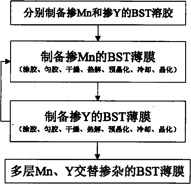
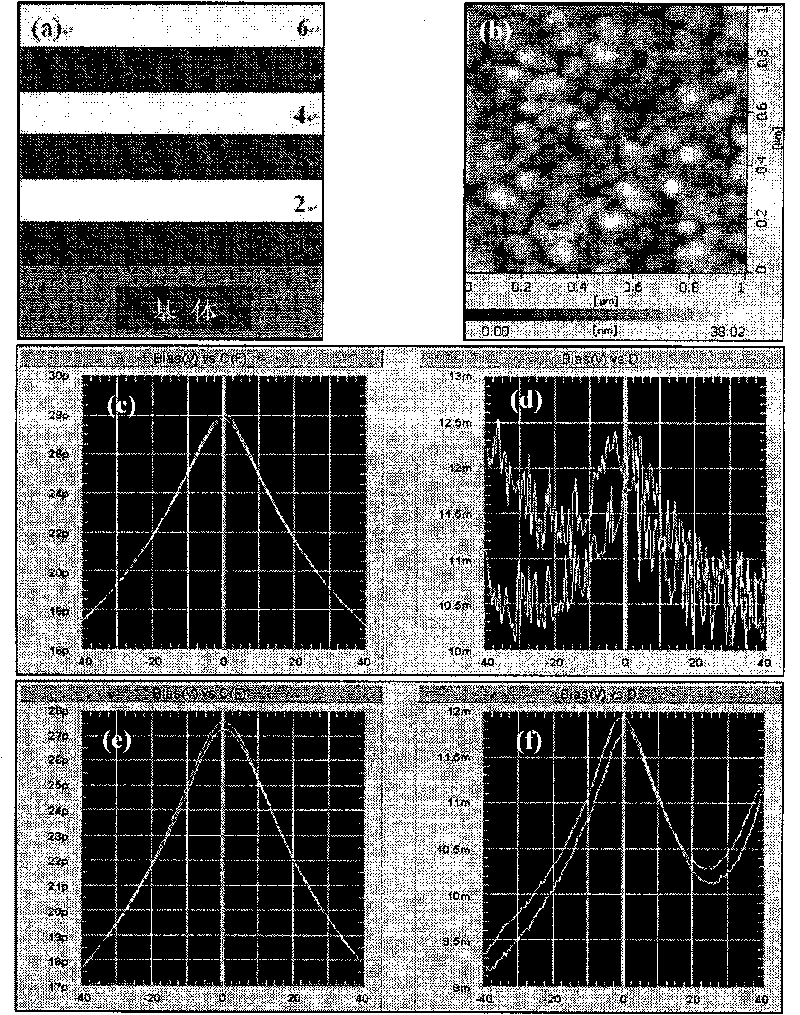
[0045] Embodiment 1 prepares Si / SiO 2 Six layers of 1mol% Mn and 1mol% Y alternately doped BST films on / Ti / Pt substrate.

[0046] According to technical scheme described in the present invention in Si / SiO 2 / Ti / Pt substrate prepared six layers of 1mol% Mn and 1mol% Y alternately doped BST thin films, such as figure 2 shown. Wherein, the doping concentration of Mn or Y refers to the percentage doping concentration relative to the molar weight of barium strontium in the BST sol (all the following examples are the same); Odd layers are doped with Mn and pre-crystallized, and even layers are doped with Y and pre-crystallized. crystallize.

[0047] The prepared BST thin film such as figure 2 , where: (a) is a schematic diagram of the film structure, (b) is the AFM morphology of the film, (c) and (d) correspond to the capacitance and dielectric loss of the film at 100kHz, respectively, (e) and (f) Corresponding to capacitance and dielectric loss at 1MHz, respectively.

[00...

Embodiment 2

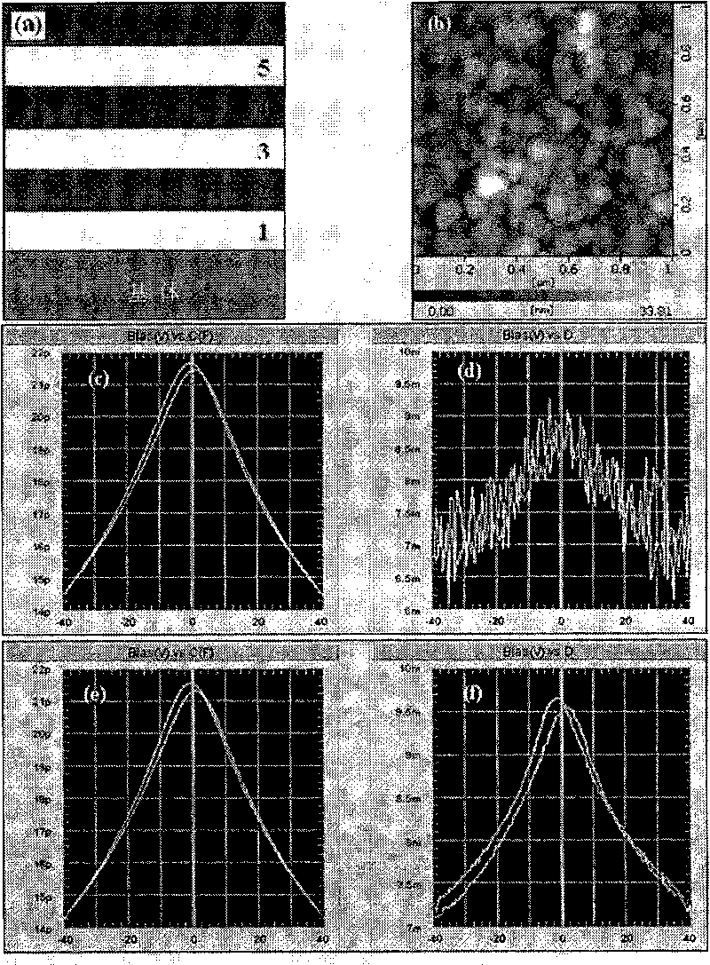
[0049] Embodiment 2 prepares Si / SiO 2 Six layers of 1mol% Y and 1mol% Mn alternately doped BST films on / Ti / Pt substrate.

[0050] According to technical scheme described in the present invention in Si / SiO 2 Six layers of 1mol% Y and 1mol% Mn alternately doped BST thin films prepared on / Ti / Pt substrate, such as image 3 shown. The odd-numbered layers are doped with Y and pre-crystallized, and the even-numbered layers are doped with Mn and pre-crystallized.

[0051] The prepared BST thin film such as image 3 , where: (a) is a schematic diagram of the film structure, (b) is the AFM morphology of the film, (c) and (d) correspond to the capacitance and dielectric loss of the film at 100kHz, respectively, (e) and (f) Corresponding to capacitance and dielectric loss at 1MHz, respectively.

[0052] Depend on image 3 It can be seen that the surface of the BST film is smooth, dense, and free of cracks, but the grain boundaries are clearer, and the average size of nanocrystal g...

Embodiment 3

[0053] Embodiment 3 prepares Si / SiO 2 Six layers of 1.5mol% Mn and 1.5mol% Y alternately doped BST films on / Ti / Pt substrate.

[0054] According to technical scheme described in the present invention in Si / SiO 2 Six layers of 1.5mol% Mn and 1.5mol% Y alternately doped BST thin films prepared on / Ti / Pt substrate, such as Figure 4 shown. The odd-numbered layers are doped with Mn and pre-crystallized, and the even-numbered layers are doped with Y and pre-crystallized.

[0055] The prepared BST thin film such as Figure 4 , where: (a) is a schematic diagram of the film structure, (b) is the AFM morphology of the film, (c) and (d) correspond to the capacitance and dielectric loss of the film at 100kHz, respectively, (e) and (f) Corresponding to capacitance and dielectric loss at 1MHz, respectively.

[0056] Depend on Figure 4 It can be seen that the surface of the BST thin film is smooth, dense and free of cracks, and the average grain size is about 50nm. At 100kHz: the ca...


PUM

PropertyMeasurementUnit
dielectric lossaaaaaaaaaa

Abstract

The invention discloses a method for preparing a binary alternatively-doped BST membrane, belongs to the technical field of functional materials, and relates to a method for preparing a nanocrystalline BST membrane. The method adopts binary doping of Mn and Y, namely, carries out Mn or Y doping on an odd layer membrane and carries out Y or Mn doping on an even layer membrane; and the method adds a pre-crystallization processing step between cooling and crystallization steps. The membrane prepared by the method is smooth and compact with no crack or shrinkage cavity, and can greatly enhance the comprehensive dielectric tuning performance of the nanocrystalline BST membrane; and the obtained nanocrystalline BST membrane has a dielectric tuning rate of over 30.0 percent, a dielectric loss of less than 2.0 percent, a K factor of greater than 15.5, a high dielectric strength and a stable frequency characteristic and a temperature characteristic. The nanocrystalline BST membrane prepared by the method can be used for preparing a microwave tuning device (such as a phase shifter) instead of a ferrite and a semiconductor so as to remarkably reduce the manufacturing cost of the microwave tuning device; and furthermore, the nanocrystalline BST membrane prepared by the method is applicable for magnetic recording, pyroelectric focal plane arrays and the like.

Description

technical field [0001] The invention belongs to the technical field of functional materials, and relates to a preparation method of a nanocrystalline barium strontium titanate (BST) thin film. Background technique [0002] BST thin film has a high dielectric tuning rate due to the nonlinear change of dielectric constant with the applied electric field, and has broad application prospects in the field of microwave devices. For example, BST thin-film phase shifters are considered as the best candidates to replace ferrite phase shifters and semiconductor diode phase shifters. However, in order to realize the application of BST films in the microwave field, in addition to high dielectric tunability, low dielectric loss and high stability are required, especially the ratio of high dielectric tunability to dielectric loss, that is, K Factor, because the K factor is an important indicator of BST comprehensive dielectric tuning performance. BST is a typical ABO 3 type perovskite ...

Claims


Application Information

Patent Timeline
Patent Type & Authority Applications(China)
IPC IPC(8): B32B9/04B82B3/00C04B35/465C04B35/22C04B41/52
Inventor 廖家轩贾宇明魏雄邦田忠傅向军张佳
Owner UNIV OF ELECTRONICS SCI & TECH OF CHINA
Why Eureka
Try Eureka