Semiconductor electrode, manufacturing method thereof and solar cell having semiconductor electrode

A technology of solar cells and semiconductors, applied in the field of dye-sensitized solar cells, which can solve problems such as cracking, shedding, and poor photoelectric conversion performance of cells

Inactive Publication Date: 2010-06-09
BYD CO LTD
View PDF0 Cites 13 Cited by
  • Summary
  • Abstract
  • Description
  • Claims
  • Application Information

AI Technical Summary

Problems solved by technology

The morphology of the sputtered deposition layer is "feather-like structure". This method can improve the bonding force between the conductive bottom layer and the porous semiconductor layer, but the feather-like sputtered deposition layer is obtained by D

Method used


Image

  • Semiconductor electrode, manufacturing method thereof and solar cell having semiconductor electrode
  • Semiconductor electrode, manufacturing method thereof and solar cell having semiconductor electrode
  • Semiconductor electrode, manufacturing method thereof and solar cell having semiconductor electrode

Examples


specific Embodiment approach

[0043] Take 3g of TiO with a particle size of 30nm 2 , 0.5g polyethylene glycol 2000 (PVA2000), 0.1mL acetylacetone, and 5mL deionized water were mixed and slowly ground, then 7mL deionized water was slowly added to it several times, after grinding for 50min, after adding 0.15mLOP emulsifier Continue grinding for 20 minutes to obtain the desired titanium dioxide slurry. The titania slurry was coated on top of the transition semiconductor layer and dried at room temperature for 24 hours. Put the dried film in a muffle furnace for sintering, raise it from room temperature to 120°C at 1°C / min, keep it for 30 minutes, then raise it to 450°C at a speed of 2°C / min, keep it for 30 minutes, anneal, and cool to The porous conductor layer can be obtained at room temperature.

[0044] The preparation method and steps of the dye layer are well known to those skilled in the art. For example, the dye layer can be formed on the porous semiconductor layer by immersing one side of the porous...

Embodiment 1

[0052] This example is used to prepare the semiconductor electrode for a dye-sensitized solar cell provided by the present invention and the dye-sensitized solar cell containing the semiconductor electrode.

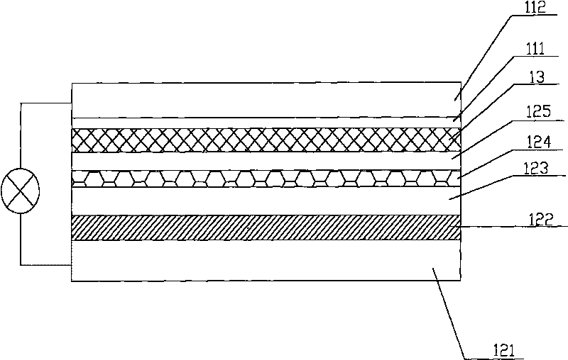
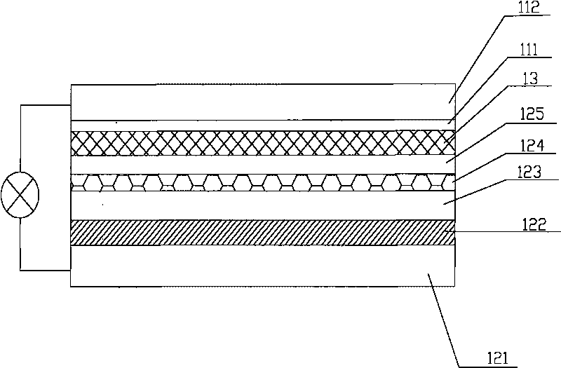
[0053] (1) Preparation of dense semiconductor layer

[0054] The conductive glass (FTO conductive glass with a square resistance of 15 ohms manufactured by Qinhuangdao Yaohua Glass Co., Ltd., with a thickness of 4 mm) coated with a fluorine-doped tin dioxide layer with a size of 3 × 1.5 cm is used as a pre-plating workpiece. With TiO2 as the evaporation source, the electron beam current is 180mA, and the vacuum degree is 1×10 -3 A dense semiconductor layer A1 with a thickness of 0.1 micron was formed on one side of the conductive bottom layer by vacuum evaporation for 5 minutes under the condition of Pa. The porosity of the dense semiconductor layer is 0.1% as detected by an automatic mercury porosimeter (Mike Instruments Inc., Auto Pore IV9500, USA).

[0055] (2) Prepa...

Embodiment 2

[0067] This example is used to prepare the semiconductor electrode for a dye-sensitized solar cell provided by the present invention and the dye-sensitized solar cell containing the semiconductor electrode.

[0068] (1) Preparation of dense semiconductor layer

[0069] The conductive glass (FTO conductive glass with a square resistance of 15 ohms manufactured by Qinhuangdao Yaohua Glass Co., Ltd., with a thickness of 4 mm) coated with a fluorine-doped tin dioxide layer with a size of 3 × 1.5 cm is used as a pre-plating workpiece. with TiO 2 As the evaporation source, the current of the electron beam is 360mA, and the degree of vacuum is 8×10 -3 Vacuum evaporation under the condition of Pa for 30 minutes forms a dense semiconductor layer A2 with a thickness of 10 microns on one side of the conductive bottom layer. The porosity of the dense semiconductor layer is 2.0% as detected by an automatic mercury porosimeter (Mike Instruments Inc., Auto Pore IV9500, USA).

[0070] (2) ...


PUM

PropertyMeasurementUnit
Diameteraaaaaaaaaa
Thicknessaaaaaaaaaa
Particle diameteraaaaaaaaaa

Abstract

The invention discloses a semiconductor electrode for a dye-sensitized solar cell, which comprises a conductive bottom layer, a compact semiconductor layer, a transitional semiconductor layer, a porous semiconductor layer and a dye layer, wherein the compact semiconductor layer, the transitional semiconductor layer, the porous semiconductor layer and the dye layer are sequentially formed on the conductive bottom layer; the compact semiconductor layer is obtained by vacuum evaporation; the transitional semiconductor layer is obtained by a sol-gel method; the porous semiconductor layer is obtained by a powder coating method; and the transitional semiconductor layer is formed between the compact semiconductor layer and the porous semiconductor layer, so the bonding force between the semiconductor electrode and the semiconductor layers is improved, and consequently the photoelectric conversion rate of the dye-sensitized solar cell is improved.

Description

technical field [0001] The invention relates to a semiconductor electrode, a preparation method thereof and a dye-sensitized solar cell containing the semiconductor electrode. Background technique [0002] Dye-sensitized solar cells, as a type of solar cells, do not require silicon as a raw material, and the more common silicon solar cells have the advantages of low cost, simple manufacturing process, and high photoelectric conversion efficiency, and have become a research hotspot in recent years. [0003] The dye-sensitized solar cell mainly includes a semiconductor electrode, a counter electrode, and an electrolyte between the semiconductor electrode and the counter electrode. The semiconductor electrode includes a conductive bottom layer, a semiconductor nanolayer formed on the conductive bottom layer, and a dye formed on the semiconductor nanolayer. layer. The working principle of the dye-sensitized solar cell is: when the dye molecule absorbs sunlight, its electrons ar...

Claims


Application Information

Patent Timeline
IPC IPC(8): H01G9/20H01G9/04H01G9/042H01G9/048H01M14/00H01L31/0224H01L31/18
CPCY02E10/542Y02P70/50
Inventor 陈炎刘倩倩林信平宫清
Owner BYD CO LTD
Why Eureka
Try Eureka