High-power gallium nitride based LED with novel structure

A gallium nitride-based, high-power technology, applied in electrical components, circuits, semiconductor devices, etc., can solve problems that restrict photoelectric conversion efficiency, and achieve the effects of small effective mass, high concentration, and increased overlap

Inactive Publication Date: 2010-06-16
SUZHOU NANOJOIN PHOTONICS
View PDF1 Cites 38 Cited by
  • Summary
  • Abstract
  • Description
  • Claims
  • Application Information

AI Technical Summary

Problems solved by technology

At the same time, because GaN series materials are polar semiconductor materials, under the action of the built-in electric field, electrons occupy the side near the p-region in a single quantum well, and holes occupy the side near the n-region. Due to the effect of

Method used


Image

  • High-power gallium nitride based LED with novel structure
  • High-power gallium nitride based LED with novel structure
  • High-power gallium nitride based LED with novel structure

Examples


Embodiment Construction

[0032] The present invention will be further described below in conjunction with accompanying drawing and embodiment:

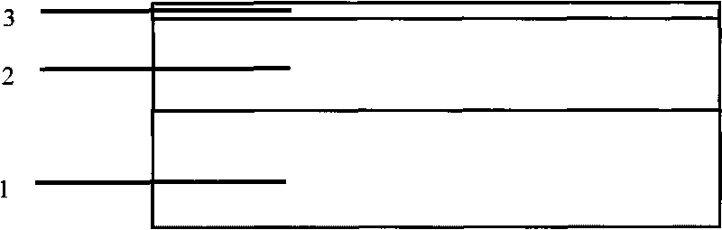
[0033] Step 1: epitaxially grow n-GaN layer 2 and AlGaN layer 3 on substrate 1 in sequence (refer to figure 1 );

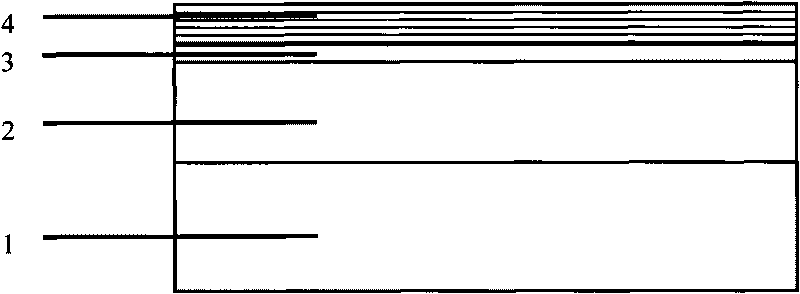
[0034] Step 2: growing the active layer 4 above the AlGaN layer 3, wherein the well width in the active region is controlled by adjusting the growth time, so that the well width gradually decreases from 3nm to 2nm from bottom to top (refer to figure 2 );

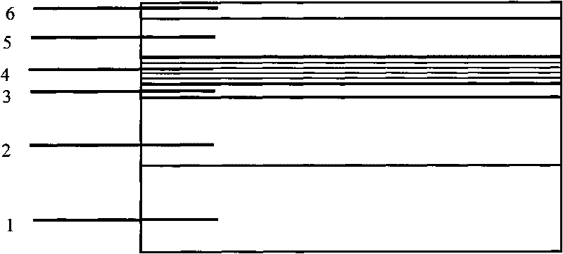
[0035] Step 3: On the active layer 4, grow p-GaN layer 5 and p+ -InGaN conductive layer 6 (refer to image 3 );

[0036] Step 4: In p + -On the InGaN layer 6, a masking layer 7 is deposited by PECVD; the material of the masking layer is SiO 2 (refer to Figure 4 );

[0037] Step 5: Coat photoresist on masking layer 7, use the method for photolithography and wet etching, carve strip-shaped n-GaN electrode region 8 on masking layer 7 (refer to Figure 5 );

[0038] Step 6: remove remain...


PUM

PropertyMeasurementUnit
Thicknessaaaaaaaaaa

Abstract

The invention relates to a gallium nitride based light-emitting diode, in particular to a high-power gallium nitride based light-emitting diode structure; the high-power gallium nitride based light-emitting diode comprises a substrate, an N-type gallium nitride layer arranged on the substrate, a AlGaN cavity barrier layer arranged on a high table top of the N-type gallium nitride layer, an asymmetrical multiple quantum well active layer arranged on the cavity barrier layer, a P-type gallium nitride layer arranged on the asymmetrical multiple quantum well active layer, a P+-InGaN conducting layer arranged on the P-type gallium nitride layer, and an indium titanium oxide electrode layer which is arranged on the P+-InGaN conducting layer from bottom to top; a silicon dioxide passivation layer is arranged on the top surface of the whole light-emitting diode and the side surface connected to the high and low table tops, an N electrode is arranged on the lower table top of the N-type gallium nitride layer, and a P-electrode is arranged in the middle of the indium titanium oxide electrode layer. The light-emitting diode structure can improve the injection efficiency of the cavity and improve the photoelectric conversion efficiency.

Description

technical field [0001] The invention relates to a gallium nitride-based light-emitting diode, in particular to a structure of a high-power gallium nitride-based light-emitting diode. Background technique [0002] Semiconductor lighting LED has significant advantages such as long life, energy saving, and environmental protection. It is considered to be another revolution in lighting technology after incandescent lamps and fluorescent lamps. It is currently the focus of research and development and industry attention in the field of semiconductors and lighting in the world, and has a huge application prospect. . [0003] The traditional structure of the existing gallium nitride-based light-emitting diodes is to use sapphire as the substrate, and then on one side of the sapphire substrate, an N-type gallium nitride contact layer, an indium gallium nitride contact layer, and an indium gallium nitride contact layer are respectively arranged from bottom to top. The light-emitting...

Claims


Application Information

Patent Timeline
IPC IPC(8): H01L33/00
Inventor 郝国栋王怀兵孔俊杰范亚明陈勇黄晓辉
Owner SUZHOU NANOJOIN PHOTONICS
Why Eureka
Try Eureka