Integration method for electric absorption modulation laser and modular spot converter

A mode spot converter and electro-absorption modulation technology, applied in lasers, laser parts, semiconductor lasers, etc., to achieve the effects of high internal quantum efficiency, reduction of Auger recombination, and reduction of growth times

Inactive Publication Date: 2007-02-07
INST OF SEMICONDUCTORS - CHINESE ACAD OF SCI
View PDF0 Cites 12 Cited by
  • Summary
  • Abstract
  • Description
  • Claims
  • Application Information

AI Technical Summary

Problems solved by technology

[0016] At present, there have been no reports on monolithic integrated devices of semiconductor DFB lasers, electroabsorption modulators and mode-spot converters in the world.

Method used


Image

  • Integration method for electric absorption modulation laser and modular spot converter
  • Integration method for electric absorption modulation laser and modular spot converter
  • Integration method for electric absorption modulation laser and modular spot converter

Examples


Embodiment

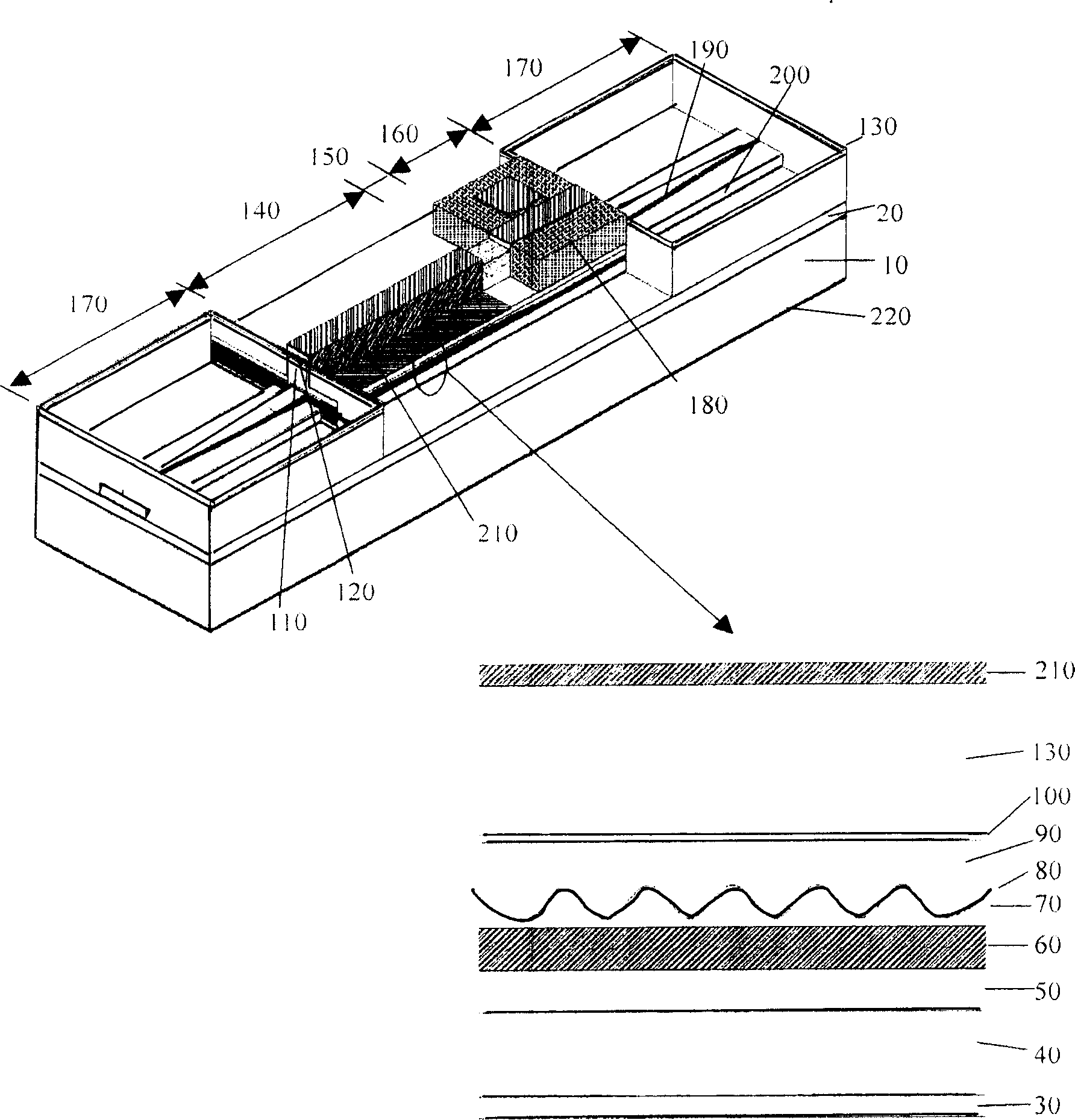
[0098] see again figure 1 As shown, the present invention relates to an integrated method of an electroabsorption modulated laser and a mode spot converter, comprising the following manufacturing steps:

[0099] (1) The 2-inch n-InP substrate undergoes strict decontamination (heating and boiling with ethanol, trichlorethylene, acetone, and ethanol in sequence) → pickling (soaking in concentrated sulfuric acid for 1 to 2 minutes) → water washing (rinsing with deionized water More than 50 times) → after drying treatment, put it into the growth chamber, the growth temperature is 655°C, the growth pressure is 22mbar, and the graphite boat rotates at 75-80 rpm. Growth rate 0.4~0.7nm / s;

[0100] (2) On the n-type indium phosphide substrate (100) epitaxially grow n-type indium phosphide buffer layer (0.5μm thick), lower waveguide layer (thickness 50nm, bandgap wavelength 1.1μm), 0.2μm phosphide Indium space layer, thin 1.1Q layer (30nm);

[0101] (3) Using PECVD technology to grow...


PUM


Abstract

The invention relates to an integration method of electric adsorption modulation laser and mode speckle converter, which comprises: growing n-type indium phosphate buffer layer on the substrate; corroding the upper 1.1Q layer on the chip, to grow buffer layer; growing silica dioxide protective layer on the whole chip, and corroding the silica dioxide protective layer at two ends of mode speckle converter; pouring low-energy phosphate ion; growing the silica dioxide protective layer again; heating, keeping warm, anneal on the chip; corroding silica dioxide protective layer; using relative light etching plate to mask the laser and modulator, to form the upper ridge and lower ridge on the converter; growing p-type indium phosphate and indium gallium arsenic phosphate etching stop layer; etching ridge pilot structure; depositing medlin at two sides of laser and modulator; opening the electrode windows of laser and modulator; etching the electrode images on the laser and modulator to splash the P electrode and remove the P electrode; extending the substrate, and splashing n electrode; slicing the sample to form tubular chip.

Description

technical field [0001] The present invention relates to an integrated method for fabricating an electroabsorption modulated laser and a mode spot converter by means of selective area growth (SAG), quantum well hybridization (QWI) and asymmetric double waveguide (ATG) technologies, using commonly used wet etching and photolithography techniques . Background technique [0002] With the development of modern information society, the high-speed transmission, processing and storage of ultra-large capacity and long-distance information is a key technology. Whether it is the backbone network of long-distance communication, wide area network, or local area network of short-distance communication, access network, short-distance data connection optical switching, etc., a large number of high-performance and low-cost optoelectronic devices are required to support the network functions. The development of monolithically integrated multifunctional photonic devices is the key to reducing...

Claims


Application Information

Patent Timeline
Patent Type & Authority Applications(China)
IPC IPC(8): H01S5/00
Inventor 侯廉平王圩朱洪亮周帆
Owner INST OF SEMICONDUCTORS - CHINESE ACAD OF SCI
Why Eureka
Try Eureka