

Heavily-doped UMG silicon epitaxially generated high-low junction-based solar cell and preparation method
A solar cell, high-low junction technology, applied in the field of solar energy applications, can solve problems such as affecting cell efficiency, polluting thin films, and reducing thin film quality
- Summary
- Abstract
- Description
- Claims
- Application Information
AI Technical Summary
Problems solved by technology
Method used
Image

Examples
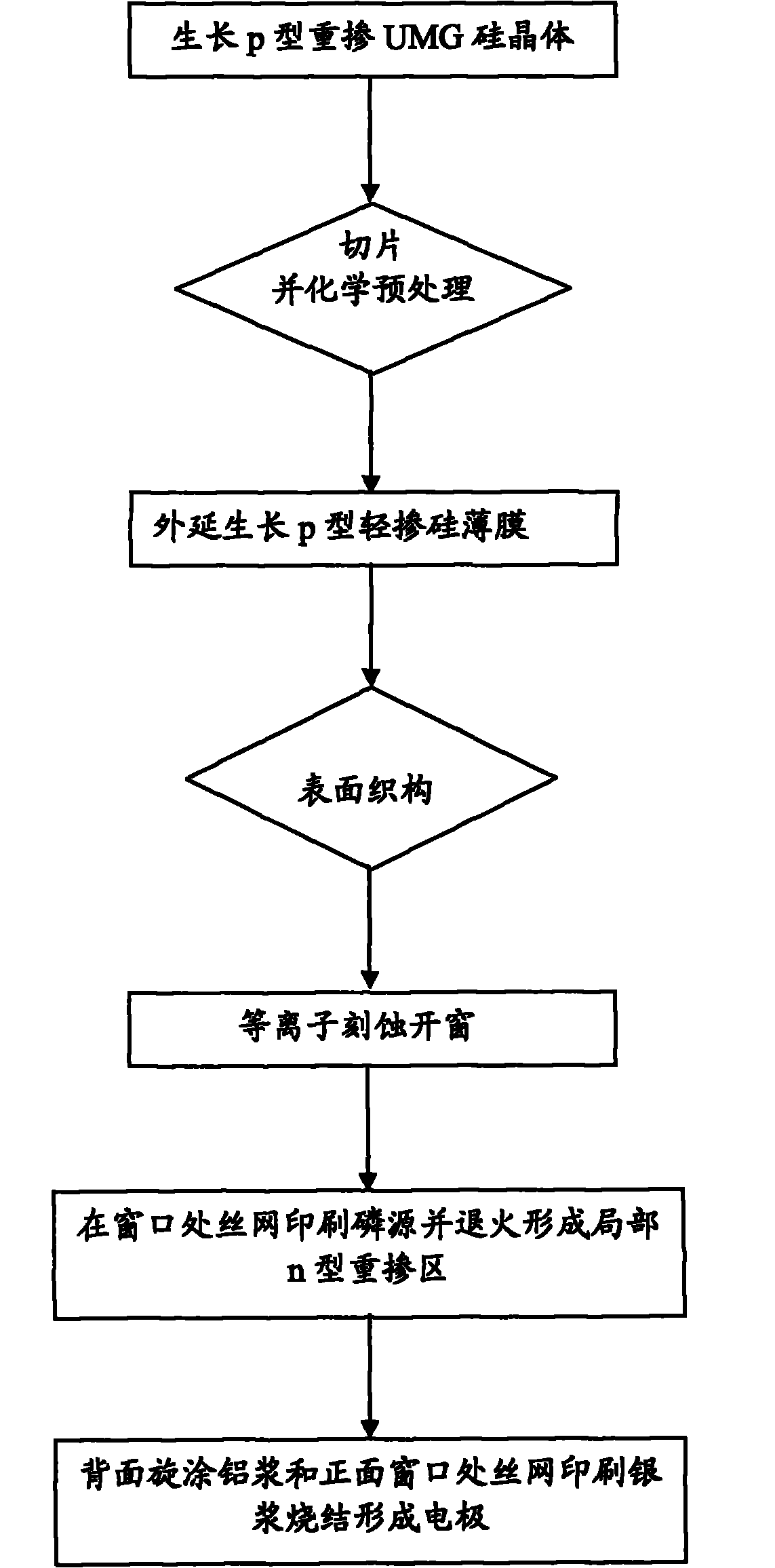
Embodiment 1
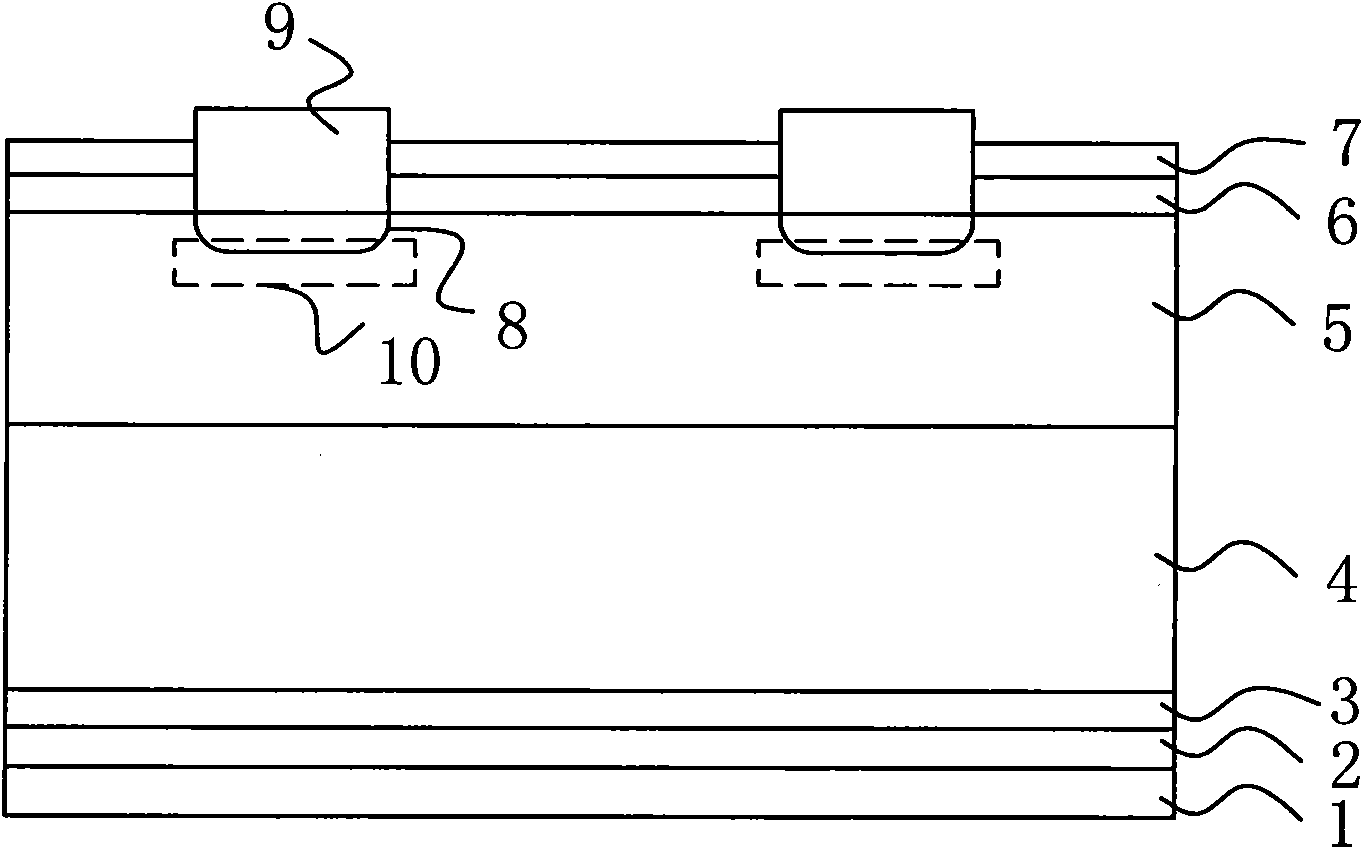
[0069] see figure 1 , the present invention is based on heavily doped UMG silicon epitaxy to generate solar cells with high and low junctions, and the order from bottom to top is as follows:
[0070] Aluminum electrode layer 1;
[0071] a first silicon nitride layer 2;
[0072] a first silicon dioxide layer 3;
[0073] Heavy doped UMG silicon layer 4, the conductivity type of this layer can be p-type or n-type;
[0074] Lightly doped silicon epitaxial layer 5, the conductivity type of this layer is the same as the conductivity type of heavily doped UMG silicon layer 4;
[0075] second silicon dioxide layer 6;
[0076] the second silicon nitride layer 7;
[0077] Wherein in the lightly doped silicon epitaxial layer 5, there are some heavily doped regions 8 distributed near the surface of the second silicon dioxide layer 6, and the conductivity type of the heavily doped regions 8 is the same as that of the heavily doped UMG silicon layer 4. type opposite;
[0078] A silve...
Embodiment 2
[0095] According to the process of Example 1, cells of heavily doped p-type UMG solar cells were prepared, the only difference being that the raw silicon ingot was polysilicon grown by directional solidification using UMG silicon, and volume A solution with a ratio of nitric acid: hydrofluoric acid: acetic acid = 3:1:10 was used for texturing.
[0096] Wherein the mass percent concentration of nitric acid is 65%, and the mass percent concentration of hydrofluoric acid is 49%.
[0097] The efficiency of the finally obtained cell reaches 15.2% (AM1.5, light intensity 100mW / cm 2 , 25℃), no light attenuation.
Embodiment 3
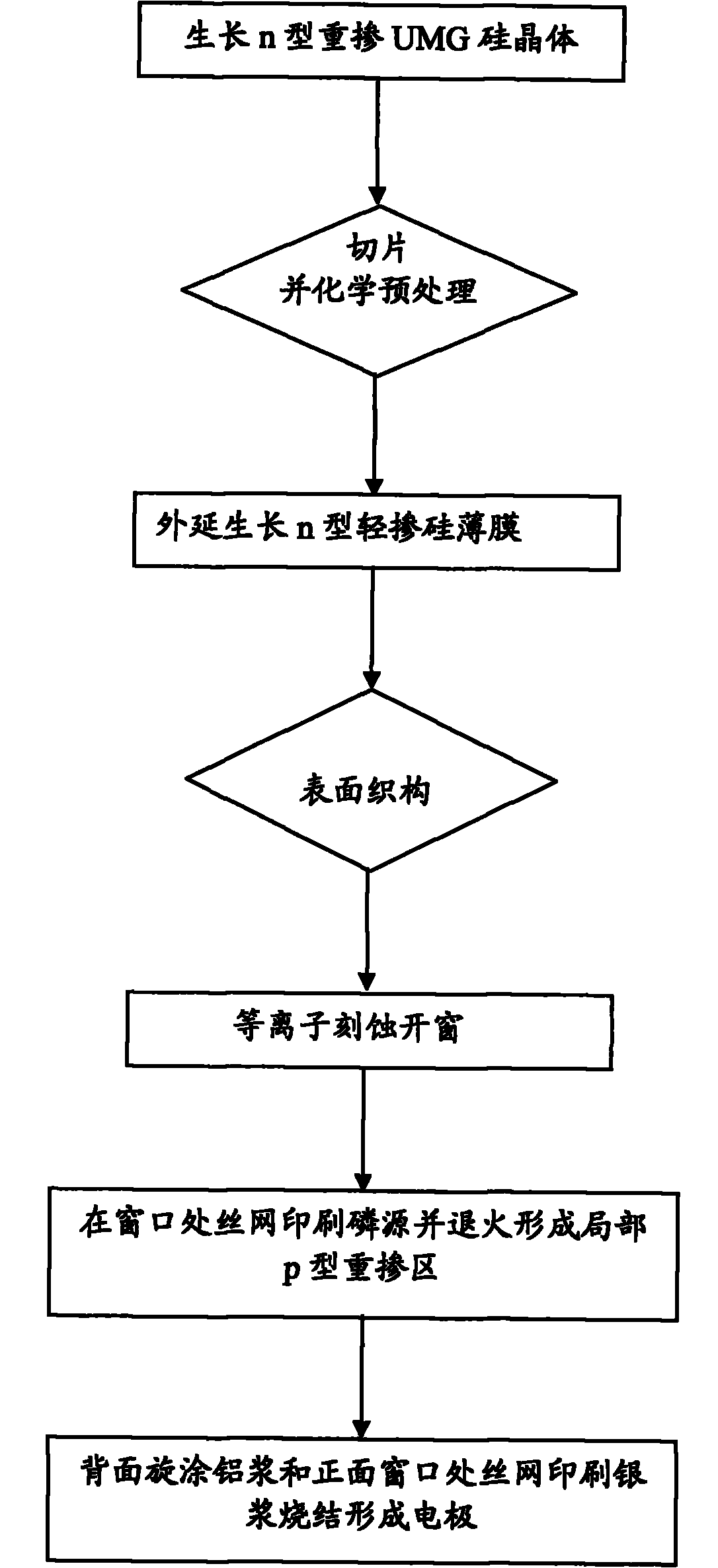
[0099] see image 3 , the process of preparing heavily doped n-type UMG solar cells is as follows:
[0100] UMG silicon is grown (100) single crystal silicon by the Czochralski method to obtain the raw silicon ingot, the dopant in the raw silicon ingot is phosphorus, and the doping concentration is 2×10 20 cm -3 .
[0101] Cut the raw silicon ingot into square slices with a thickness of 150 μm; mechanically polish the slices until their surface is bright, use conventional semiconductor cleaning processes to clean, chemically polish, wash with deionized water several times, and dry with infrared lamps to obtain UMG silicon wafers .
[0102] UMG silicon wafer is used as the substrate, and lightly doped silicon epitaxial layer is grown on the surface of UMG silicon wafer by CVD technology to obtain semi-finished cells. The thickness of the lightly doped silicon epitaxial layer is 25 μm, and the dopant in the lightly doped silicon epitaxial layer is POCl 3 , with a doping conc...
PUM
 Abstract
Description
Claims
Application Information