Preparation method of MEMS microbridge structure

A technology of micro-bridge structure and sacrificial layer, which is applied in the direction of micro-structure technology, micro-structure device, manufacturing micro-structure device, etc., can solve the problems of small process window, poor electrical characteristics of aluminum pillars, high aluminum resistivity, etc., and reduce the process Effects of complexity, improved performance, and reduced wiring resistance

Active Publication Date: 2010-07-21
SHANGHAI INTEGRATED CIRCUIT RES & DEV CENT +1
View PDF5 Cites 19 Cited by
  • Summary
  • Abstract
  • Description
  • Claims
  • Application Information

AI Technical Summary

Problems solved by technology

However, this process has some obvious disadvantages. Especially in the process of making aluminum pillar metal, the etching of aluminum requires the process to stop on the sensitive material layer. The process steps are complicated and the process control is difficult, resulting in a relatively large subsequent process window. Small, not conducive to the subsequent process
In addition, due to the high resistivity of aluminum, the electrical characteristics of aluminum pillars are also poor.

Method used


Image

  • Preparation method of MEMS microbridge structure
  • Preparation method of MEMS microbridge structure
  • Preparation method of MEMS microbridge structure

Examples


Embodiment Construction

[0019] In order to make the object, technical solution and advantages of the present invention clearer, the present invention will be further described in detail below in conjunction with the accompanying drawings.

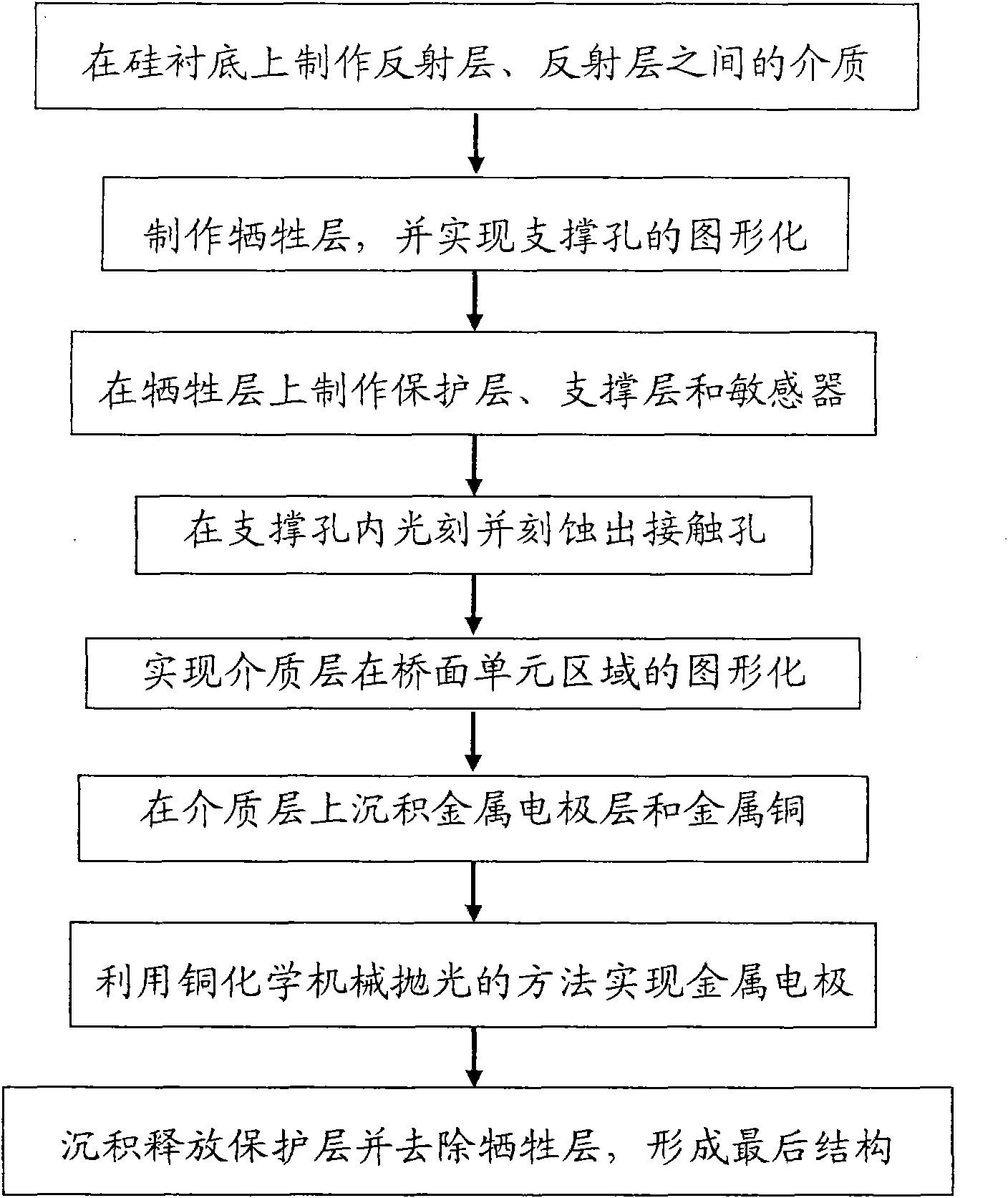
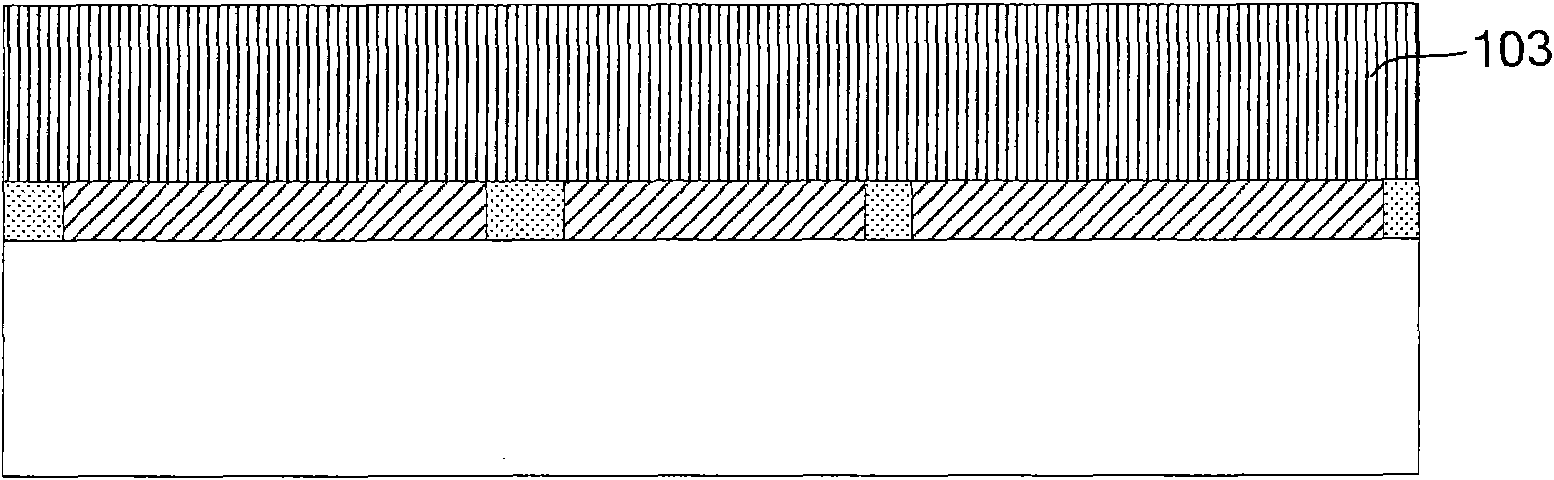
[0020] This embodiment provides a method for preparing a MEMS microbridge structure, such as figure 1 Shown is the flow chart of the method for preparing the MEMS microbridge structure of the present invention. to combine Figure 2 to Figure 11 MEMS microbridge structure preparation method of the present invention comprises the following steps:

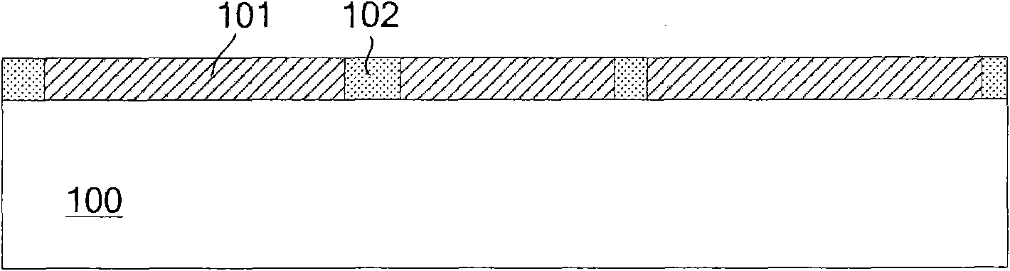
[0021] Step 1, fabricate the reflective layer 101 and the medium 102 between the reflective layers on the substrate 100, such as figure 2 As shown, in this embodiment, the substrate 100 is selected as a silicon substrate, but it is not limited to semiconductor substrates such as silicon, and non-semiconductor substrates such as glass substrates can also be applied to this embodiment. The reflective layer 101 It is met...


PUM


Abstract

The invention provides a preparation method of an MEMS microbridge structure. The method comprises the following steps: 1. preparing a reflecting layer on the surface area of a substrate; 2. preparing a sacrificial layer on the surface area of the reflecting layer, etching a supporting hole on the sacrificial layer; 3. successively preparing a supporting layer, a sensitive layer and a medium layer on the surface area of the sacrificial layer; 4. patterning the inside of the supporting hole and the bridge surface area, forming a contact hole; 5. depositing a metal electrode layer and metal copper on the surface area of the medium layer, flattening metal copper until the medium layer; and 6. removing the sacrificial layer and forming the finished microbridge structure. The preparation method uses the copper pillar instead of the traditional aluminum pillar and utilizes the copper chemical-mechanical polishing method to realize the self-alignment patterning of the metal electrode so that the planarization of the microbridge structure can be realized, the connection resistance can be effectively reduced and the complexity of the process can also be reduced.

Description

technical field [0001] The invention relates to a MEMS micro-bridge structure, in particular to a method for preparing the MEMS micro-bridge structure. Background technique [0002] Micro-Electro-Mechanical System (MEMS) technology can integrate mechanical components, drive components, electronic control systems, digital processing systems, etc. into a micro-system as an overall unit. This kind of MEMS can not only collect, process and send information or instructions, but also take actions independently or according to external instructions according to the acquired information. It uses the combination of microelectronics technology and micromachining technology (including micromachining of silicon body, micromachining of silicon surface, LIGA and wafer bonding and other technologies) to manufacture various sensors with excellent performance, low price and miniaturization. Actuators, drives and microsystems. It has many advantages such as tiny, intelligent, executable, in...

Claims


Application Information

Patent Timeline
Patent Type & Authority Applications(China)
IPC IPC(8): B81C1/00
Inventor 康晓旭姜利军蒋宾赵宇航池积光钱良山庞惠民
Owner SHANGHAI INTEGRATED CIRCUIT RES & DEV CENT
Why Eureka
Try Eureka