Etching solution for processing N-type silicon microchannel array by photon-assisted electrochemical etching method

A silicon microchannel, electrochemical technology, applied in the field of etching solution, can solve the problems of silicon microchannel pore size becoming larger, difficult to control, difficult to obtain a large aspect ratio silicon microchannel structure, etc.

Inactive Publication Date: 2010-08-04
CHANGCHUN UNIV OF SCI & TECH
View PDF4 Cites 2 Cited by
  • Summary
  • Abstract
  • Description
  • Claims
  • Application Information

AI Technical Summary

Problems solved by technology

Side etching leads to the gradual enlargement of the pore size of the formed silicon microchannel, which is difficult to control
The longer t

Method used


Image

  • Etching solution for processing N-type silicon microchannel array by photon-assisted electrochemical etching method
  • Etching solution for processing N-type silicon microchannel array by photon-assisted electrochemical etching method
  • Etching solution for processing N-type silicon microchannel array by photon-assisted electrochemical etching method

Examples


Embodiment 1

[0009] The preparation raw material of corrosion solution: take 200ml 40wt% hydrofluoric acid, 180ml absolute ethanol, 1800ml deionized water, mix to obtain hydrofluoric acid, ethanol aqueous solution, in this aqueous solution, the concentration of hydrofluoric acid is 4.30wt%, and the concentration of ethanol is 6.53 % by weight; additionally add 10ml of AOS, ie sodium α-olefin sulfonate, as anionic surfactant, the addition amount is 0.46% of the volume of the hydrofluoric acid and ethanol aqueous solution.

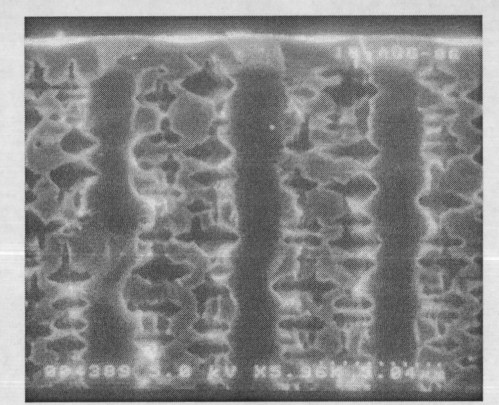
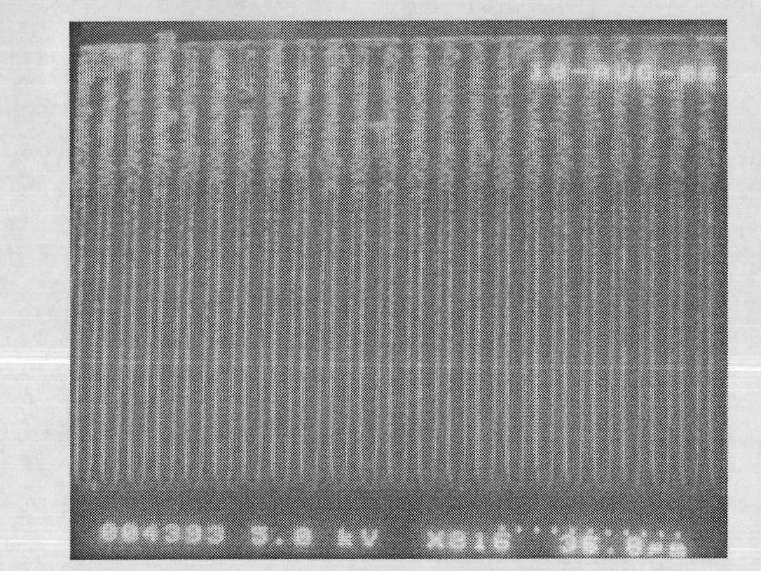
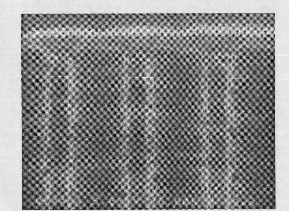
[0010] Processing of the silicon microchannel array: the light source adopts an area array of light-emitting diodes with a wavelength of 850nm and a size of 18×18, and the total power is 32.4W. The silicon wafer is an N-type crystalline silicon wafer with a resistivity of 2-4Ωcm. Under the irradiation of the light source, the holes required for the corrosion reaction are excited, anodized for 10 hours, and the average etching rate is 32 μm / hour, and a silicon microchann...

Embodiment 2

[0012] The preparation raw material of corrosion solution: take 220ml 40wt% hydrofluoric acid, 180ml absolute ethanol, 1800ml deionized water, mix to obtain hydrofluoric acid, ethanol aqueous solution, in this aqueous solution, the concentration of hydrofluoric acid is 4.68wt%, and the concentration of ethanol is 6.46 wt%; Add 20ml of AES in addition, i.e. fatty alcohol polyoxyethylene ether sodium sulfate, as anionic surfactant, the addition amount is 0.91% of the volume of the hydrofluoric acid and ethanol aqueous solution.

[0013] Processing of the silicon microchannel array: the light source adopts an area array of light-emitting diodes with a wavelength of 850nm and a size of 18×18, and the total power is 32.4W. The silicon wafer is an N-type crystalline silicon wafer with a resistivity of 2-4Ωcm. Under the irradiation of the light source, the holes required for the corrosion reaction are excited, anodized for 10 hours, and the etching rate is 34.5 μm / hour, and a macrop...


PUM

PropertyMeasurementUnit
Resistivityaaaaaaaaaa

Abstract

The invention relates to an etching solution for processing an N-type silicon microchannel array by a photon-assisted electrochemical etching method, which belongs to the technical field of silicon micro-processing. In the prior art, the etching solution for processing an N-type silicon microchannel array by a photon-assisted electrochemical etching method is made by adding ethanol or p-octyl polyethylene glycol phenyl ether, which is used as a surfacetant, into hydrofluoric acid electrolyte, and the etching solution can result in severe lateral erosion in the etching process. The etching solution of the invention is prepared from hydrofluoric acid and ethanol water solution, wherein the concentration of the hydrofluoric acid is 1-10 wt%, and the concentration of the ethanol is5-10 wt%. In addition, an anionic surfactant is added, and the amount of the anionic surfactant is 0.1-1% of the hydrofluoric acid and ethanol water solution by volume. The invention is used for processing N-type macro-pore silicon microchannel arrays.

Description

technical field [0001] The invention relates to an etching solution for processing N-type silicon microchannel arrays by a light-assisted electrochemical etching method, which is used for processing N-type macroporous silicon microchannel arrays, and belongs to the technical field of silicon microprocessing. Background technique [0002] Light-assisted electrochemical etching is a technique that can be used in the processing of N-type silicon microchannels. In N-type silicon, holes are minority carriers, and the main carriers are electrons. To make the anodic oxidation and dissolution reaction of silicon proceed, holes must be excited by light irradiation. This process is called photoelectrochemical corrosion (PEC). The silicon microchannel array is processed by light-assisted electrochemical etching method, the radial size of the silicon microchannel is 0.1-10 microns, and the depth can reach hundreds of microns. Silicon microchannel arrays have broad application prospects...

Claims


Application Information

Patent Timeline
IPC IPC(8): B81B1/00B81C1/00C25F3/12H01L21/3063
Inventor 王国政付申成端木庆铎
Owner CHANGCHUN UNIV OF SCI & TECH
Why Eureka
Try Eureka