Nano-electromechanical structure and method for the production thereof

A mechanical and microelectronic technology, applied in the direction of nanostructure manufacturing, microelectronic microstructure devices, nanotechnology, etc., can solve problems such as aggravation, unresolved devices, and reduced time stability of memory components

Inactive Publication Date: 2010-08-04
S·V·哈特夫 +1
View PDF10 Cites 2 Cited by
  • Summary
  • Abstract
  • Description
  • Claims
  • Application Information

AI Technical Summary

Problems solved by technology

In addition, the problem of charge leakage due to tunneling is exacerbated, among other problems, which reduce the temporal stability of the developed memory elements
However, in these cases, the developers have already used the potential of self-organization processes before even considering the fabrication of nanotubes, at various stages in the production of structures or by switching to conventional flat plates with very limited capacity. typography, or simply do not solve the problems encountered in forming the device of the proposed structure

Method used


Image

  • Nano-electromechanical structure and method for the production thereof
  • Nano-electromechanical structure and method for the production thereof
  • Nano-electromechanical structure and method for the production thereof

Examples


Embodiment

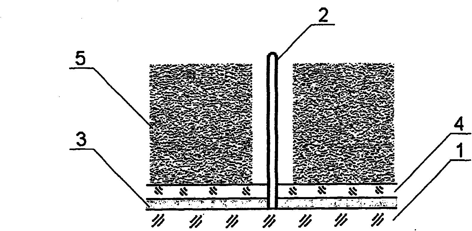
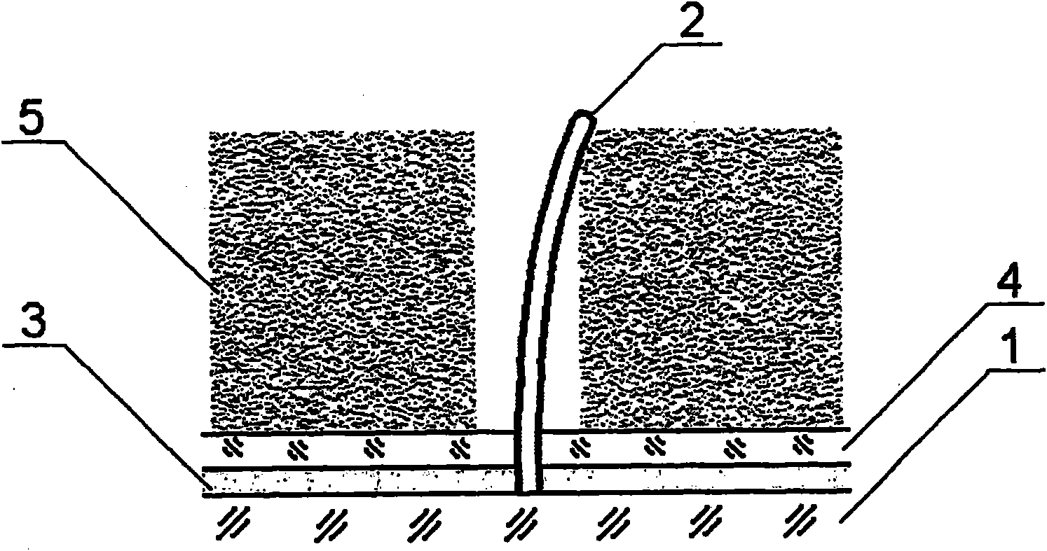
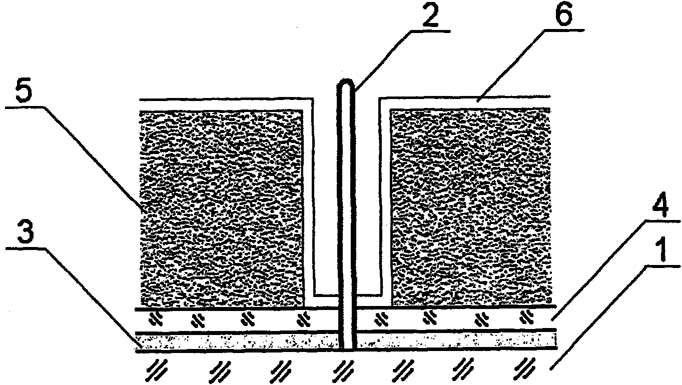
[0107] By using the sol technique, it is possible to build on a dielectric substrate 1( Figure 6) formed on the surface of nickel nanoparticles. The process of producing carbon nanotubes in an electric field is accomplished by catalytic cracking of vapors of carbon-carrying gases such as butane-propane mixtures. As a result of the process described, a large number of vertically oriented carbon nanotubes 2 is produced. The metal layer 3 (eg tantalum layer) is applied by laser ablation or sputtering. The layer performs the function of the input electrode, which also provides additional support for the nanotubes in vertical position. A dielectric layer 4 (eg aluminum oxide layer) is applied by magnetron sputtering. The amorphous carbon layer 5 is applied by sputtering, said layer performing the function of the output electrode. The electrical conductivity of the amorphous carbon layer 5 is increased by means of thermal annealing. A voltage difference of at least 3 V is appl...


PUM


Abstract

The invention relates to micro- and nano-electromechanical devices and to a method for the production thereof. One of the variants of the inventive method for producing a nano-electromechanical structure is based on the use of self-organising and self-alignment mechanisms, thereby unlimiting the substantial geometrical parameters thereof with respect to possibilities of traditional lithography, which makes it possible to achieve an integration degree equal to 1016 m-2 and greater. Moreover, one of the inventive aspects uses the resonance frequency of the elements in the form of an independentaddressing co-ordinate thereof,thereby making it possible to reduce the density of the required interconnections. The other aspect of the invention provides a gas sensor exhibiting a high sensitivityof the measurement of given gases or particles in the atmosphere, having multipurpose and flexible selectivity mechanisms and a controllable process of sensory ability regeneration. The inventive structure provides a simple method for measuring the resonance frequency of an oscillating element, which does not require high-frequency signal analysis.

Description

technical field [0001] The invention relates to micro-electromechanical and nano-electromechanical devices used in microelectronics, microsystems and sensor technology, and also to methods for their production. Background technique [0002] The potential of using nanostructures as functional elements is difficult to limit. For example, one interesting use of nanostructures is as the basis for mechanical resonators in signal processing systems. The resonator can replace the external circuitry of an integrated circuit filter based on a relatively bulky quartz resonator. The development trend of MEMS resonators (based on microelectromechanical systems) is based on the utilization of mechanical motion of suspended silicon beams. However, the typical dimensions of silicon beams correspond to the micrometer range, which dictates a natural oscillation frequency on the order of several megahertz. At higher frequencies, the quality factor (Q-factor) of such resonators begins to de...

Claims


Application Information

Patent Timeline
Patent Type & Authority Applications(China)
IPC IPC(8): B82B1/00B82B3/00
CPCG01N2291/0256B81B2201/0214G01N29/036B81C2201/0149B81B7/04B82Y30/00
Inventor S·V·哈特夫V·K·涅沃林M·M·西穆宁
Owner S·V·哈特夫
Why Eureka
Try Eureka