Method for preparing nano-structured matrix on surface of uneven substrate

A nanostructure and substrate surface technology, applied in the field of nanotechnology, can solve the problems that the exposure system cannot be micro-nano-processed on non-flat surfaces, cannot accurately control the position and force, and the processing of hard film masks is difficult. Effects of acid-base stability and thermal stability, convenient desorption and transfer, and avoidance of diffraction problems

Inactive Publication Date: 2012-05-23
UNIV OF SCI & TECH OF CHINA
View PDF0 Cites 0 Cited by
  • Summary
  • Abstract
  • Description
  • Claims
  • Application Information

AI Technical Summary

Problems solved by technology

In order to solve the defect that ordinary exposure systems cannot perform micro-nano processing on non-flat surfaces, some research groups have invented some other alternative methods, such as etching nano-patterns on hard films and then metal deposition, or through soft stamping. embossing, etc.
However, these methods also have some disadvantages, such as hard film masks are difficult to process, easily broken, and the diffraction effect caused by non-close contact is very obvious; while the soft stamp method can be used when processing nanostructures Limited material and incapable of precise position and force control

Method used


Image

  • Method for preparing nano-structured matrix on surface of uneven substrate
  • Method for preparing nano-structured matrix on surface of uneven substrate
  • Method for preparing nano-structured matrix on surface of uneven substrate

Examples


Embodiment 1

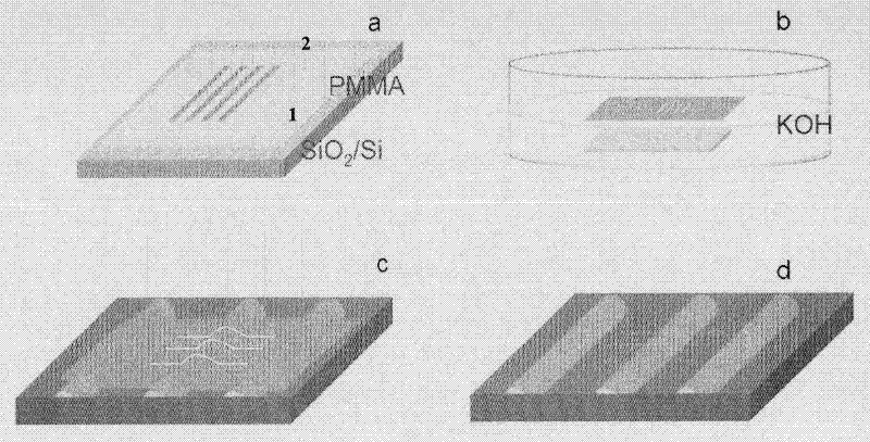
[0030] 1) Combine Si and SiO 2 Composite substrate composed of (wherein, the lattice orientation of Si sheet is 111, SiO 2 The thickness of the layer is 300 nanometers) and cut into small pieces of 1 cm×1 cm, ultrasonicated through acetone, absolute ethanol, and deionized water for five minutes respectively, and dried with nitrogen gas for later use. Mark the above-mentioned small piece of silicon wafer as substrate A.

[0031] On the substrate A, it is 671.06 PMMA (the weight average molecular weight is 950K) chloroform solution (mass percentage concentration is 6%) with the speed spin-coating model of 4000 revs / second on the substrate A, hot stage 180 ℃ glue-baking 4 minutes, obtain thickness 600 nm photoresist layer.

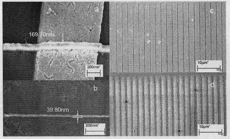
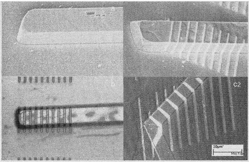
[0032] 2) The sample A that is spin-coated with PMMA is put into the electron beam exposure machine (Raith e Line), under the acceleration voltage of 15KV, with 150uAS / cm 2 Dose exposure to get a pre-designed pattern, develop for 90 seconds, and fix for on...

Embodiment 2

[0039] 1) Combine Si and SiO 2 Composite substrate composed of (wherein, the lattice orientation of Si sheet is 111, SiO 2 The thickness of the layer is 300 nanometers) and cut into small pieces of 1 cm×1 cm, ultrasonicated through acetone, absolute ethanol, and deionized water for five minutes respectively, and dried with nitrogen gas for later use. Mark the above-mentioned small piece of silicon wafer as substrate A.

[0040] After the chloroform solution (mass percentage concentration is 1%) of the PMMA (weight average molecular weight is 495K) of 671.06 PMMA (weight average molecular weight) with the speed spin-coating model of 2000 rev / s on substrate A, hot stage 180 ℃ of glue-baking 2 minutes, obtain A photoresist layer with a thickness of 120 nm.

[0041] 2) Put the sample A which is spin-coated with PMMA into the electron beam exposure machine (Raith e_Line), under the acceleration voltage of 10KV, with 100uAS / cm 2 Dose exposure to get a pre-designed pattern, 60 sec...

Embodiment 3

[0048] 1) Combine Si and SiO 2 Composite substrate composed of (wherein, the lattice orientation of Si sheet is 111, SiO 2 The thickness of the layer is 300 nanometers) and cut into small pieces of 1 cm×1 cm, ultrasonicated through acetone, absolute ethanol, and deionized water for five minutes respectively, and dried with nitrogen gas for later use. Mark the above-mentioned small piece of silicon wafer as substrate A.

[0049] After the chloroform solution (mass percentage concentration is 6%) of the PMMA (weight average molecular weight is 950K) of 671.06 PMMA (weight average molecular weight is 6%) with the speed spin coating model of 2000 rev / s on substrate A, hot stage 180 ℃ of glue-baking 4 minutes, obtain Photoresist layer with a thickness of 600 nm.

[0050] 2) The sample A that is spin-coated with PMMA is put into the electron beam exposure machine (Raith e_Line), under the accelerating voltage of 15KV, with 150uAS / cm 2 Dose exposure to get a pre-designed pattern, ...


PUM

PropertyMeasurementUnit
thicknessaaaaaaaaaa
thicknessaaaaaaaaaa
thicknessaaaaaaaaaa

Abstract

The invention discloses a method for preparing a nano-structured matrix on the surface of an uneven substrate. The method comprises the following steps: 1) coating an organic solution of a photoresist on the substrate and drying the organic solution to obtain the dried photoresist; 2) exposing, developing and fixing the dried photoresist in sequence to obtain a mask plate; 3) under the condition of a pH value of 11 to 14, hydrolyzing the mask plate to obtain a suspended mask plate, and cleaning the suspended mask plate; 4) picking up the suspended mask plate by using the substrate with an uneven surface, drying the suspended mask plate, and depositing target materials; and 5) removing the mask plate to obtain the nano-structured matrix on the substrate with the uneven surface. In the method, a PMMA film is used as a soft mask plate due to the flexibility and is closely combined with the target substrate with the uneven surface; pre-designed nano structures of specified materials can be obtained on the substrate with the uneven surface by decomposing specified nano materials; and the PMMA soft mask plate can still be reused.

Description

technical field [0001] The invention belongs to the field of nanometer science and technology, and relates to a method for preparing a nanostructure matrix on the surface of a non-flat substrate. Background technique [0002] In order to precisely control the size and shape of the prepared nanostructures, many top-down methods for preparing nanostructures have been invented, such as ultraviolet deep ultraviolet exposure system, X-ray exposure system, electron beam exposure system, ion beam direct writing system etc. However, the traditional exposure system generally requires the substrate to have a smooth and flat surface due to the requirement of photoresist leveling and flatness or the requirement of focusing rays used for exposure, and it cannot be used on non-flat substrates such as cylinders and regular triangular cylinders. Micro-nanofabrication on the bottom. [0003] In many optical devices and some electronic devices, micro-nanofabrication of curved surfaces is a ...

Claims


Application Information

Patent Timeline
Patent Type & Authority Patents(China)
IPC IPC(8): G03F7/00
Inventor 蔡洪冰张琨于欣欣王晓平
Owner UNIV OF SCI & TECH OF CHINA
Why Eureka
Try Eureka