Silicon quantum dot solar cell and preparation method thereof

A technology of solar cells and silicon quantum dots, applied in circuits, electrical components, photovoltaic power generation, etc., can solve the problems of high cost, many materials, light-induced attenuation effect, etc. simple effect

Inactive Publication Date: 2010-09-15
TSINGHUA UNIV
View PDF1 Cites 11 Cited by
  • Summary
  • Abstract
  • Description
  • Claims
  • Application Information

AI Technical Summary

Problems solved by technology

[0008] The purpose of the present invention is to overcome the shortcomings of the first generation of crystalline silicon solar cells, which have many materials and high cost, and the second generation of thin film cells have low conversion efficiency and easy to produce light-induced attenuation e...

Method used


Image

  • Silicon quantum dot solar cell and preparation method thereof
  • Silicon quantum dot solar cell and preparation method thereof
  • Silicon quantum dot solar cell and preparation method thereof

Examples


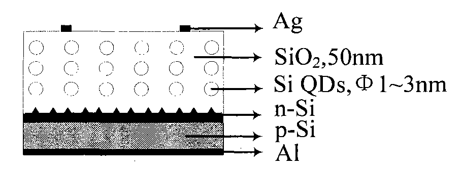
Embodiment 1

[0051] Prepare p-type (100) crystalline silicon with a thickness of 200um, and its boron doping concentration is 10 15 cm -3 , with a resistivity of 5 ohm cm, used as a substrate after cleaning with a standard semiconductor process;

[0052] On the p-type crystalline silicon substrate, sodium silicate Na with a mass fraction of 1.6% 2 SiO 3 , Sodium hydroxide NaOH with a mass fraction of 2.0% and isopropanol IPA solution with a volume fraction of 6% for texturing, that is, a water bath at 78°C to 83°C for 25 minutes to form a surface pyramid structure with a height of 6um to 8um to reduce the solar cell Surface reflectivity, increase the absorption coefficient of sunlight;

[0053] Diffusion of phosphorus oxychloride on the p-type crystalline silicon substrate to form a phosphorus concentration of 10 15 cm -3 The n-type layer;

[0054] Using PVD, that is, magnetron sputtering, a silicon monoxide film with a thickness of 50nm is prepared on the substrate with a silicon mo...

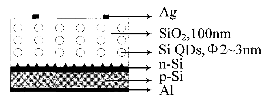
Embodiment 2

[0060] Prepare p-type (100) crystalline silicon with a thickness of 200um, and its boron doping concentration is 10 15 cm -3 , with a resistivity of 5 ohm cm, used as a substrate after cleaning with a standard semiconductor process;

[0061] On the p-type crystalline silicon substrate, sodium silicate Na with a mass fraction of 1.6% 2 SiO 3 , Sodium hydroxide NaOH with a mass fraction of 2.0% and isopropanol IPA solution with a volume fraction of 6% for texturing, that is, a water bath at 78°C to 83°C for 25 minutes to form a surface pyramid structure with a height of 6um to 8um to reduce the solar cell Surface reflectivity, increase the absorption coefficient of sunlight;

[0062] Diffusion of phosphorus oxychloride on the p-type crystalline silicon substrate to form a phosphorus concentration of 10 15 cm -3 The n-type layer;

[0063] Using PVD, that is, magnetron sputtering, a silicon monoxide film with a thickness of 100nm is prepared on the substrate with a silicon m...

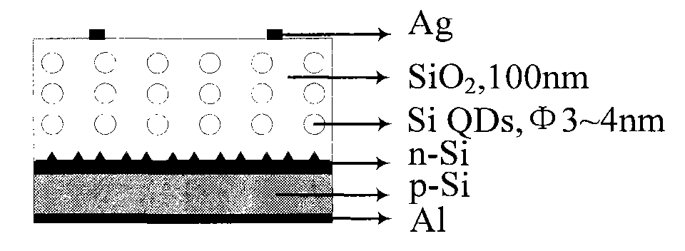
Embodiment 3

[0069] Prepare p-type (100) crystalline silicon with a thickness of 200um, and its boron doping concentration is 10 15 cm -3 , with a resistivity of 5 ohm cm, used as a substrate after cleaning with a standard semiconductor process;

[0070] On the p-type crystalline silicon substrate, sodium silicate Na with a mass fraction of 1.6% 2 SiO 3 , Sodium hydroxide NaOH with a mass fraction of 2.0% and isopropanol IPA solution with a volume fraction of 6% for texturing, that is, a water bath at 78°C to 83°C for 25 minutes to form a surface pyramid structure with a height of 6um to 8um to reduce the solar cell Surface reflectivity, increase the absorption coefficient of sunlight;

[0071] Diffusion of phosphorus oxychloride on the p-type crystalline silicon substrate to form a phosphorus concentration of 10 15 cm -3 The n-type layer;

[0072] Using PVD, that is, the method of magnetron sputtering, a silicon monoxide film with a thickness of 100nm is prepared on the substrate wi...


PUM

PropertyMeasurementUnit
Average heightaaaaaaaaaa
Thicknessaaaaaaaaaa
Thicknessaaaaaaaaaa

Abstract

The invention relates to a novel silicon quantum dot solar cell which belongs to the field of solar cells and is characterized in that a silicon quantum dot layer is added on a pn junction of a traditional crystalline silicon cell. The structure of the solar cell is as follows: phosphorus oxychloride (or boron tribromide) is diffused on a napped p type (or n type) crystalline silicon substrate, then a silicon dioxide layer containing n type (or p type) silicon quantum dots is prepared, silver positive electrodes are finally respectively added on the front surface and the back surface, and an aluminum back surface field of a silver aluminum back electrode is embedded. The cell has simple structure, strong light absorption capacity and large photo-generated current, and the preparation steps are compatible with the preparation process of the existing crystalline silicon solar cell, thereby providing a good solution way for improving the conversion efficiency of the existing crystalline silicon cell.

Description

technical field [0001] The invention relates to a solar cell and its preparation technology, in particular to two novel silicon quantum dot solar cell structures and a preparation method thereof, and belongs to the technical field of solar cells and nanomaterial applications. Background technique [0002] Solar cells are semiconductor devices with photoelectric conversion efficiency based on semiconductor materials. When n-type and p-type semiconductors are combined to form a pn junction, due to the diffusion of majority carriers, a space charge region is formed, and an ever-increasing built-in electric field from n-type to p-type is formed, resulting in a majority load The reverse drift of the current reaches equilibrium. If light shines on the pn junction, and the light energy is greater than the forbidden band width of the pn junction, electron-hole pairs will be generated near the pn junction. Due to the existence of the built-in electric field, the generated non-equil...

Claims


Application Information

Patent Timeline
IPC IPC(8): H01L31/042H01L31/0248H01L31/18
CPCY02E10/52Y02E10/50Y02P70/50
Inventor 王敬韩李豪
Owner TSINGHUA UNIV
Why Eureka
Try Eureka