Groove MOS (Metal Oxide Semiconductor) device integrating Schottky diodes in unit cell and manufacture method
A technology of Schottky diodes and MOS devices, which is applied in the manufacture of semiconductor/solid-state devices, electric solid-state devices, semiconductor devices, etc., can solve the problems of high cost, large chip area and complex process, and achieves saving silicon surface area and reducing The effect of chip cost
- Summary
- Abstract
- Description
- Claims
- Application Information
AI Technical Summary
Problems solved by technology
Method used
Image

Examples
Embodiment 1
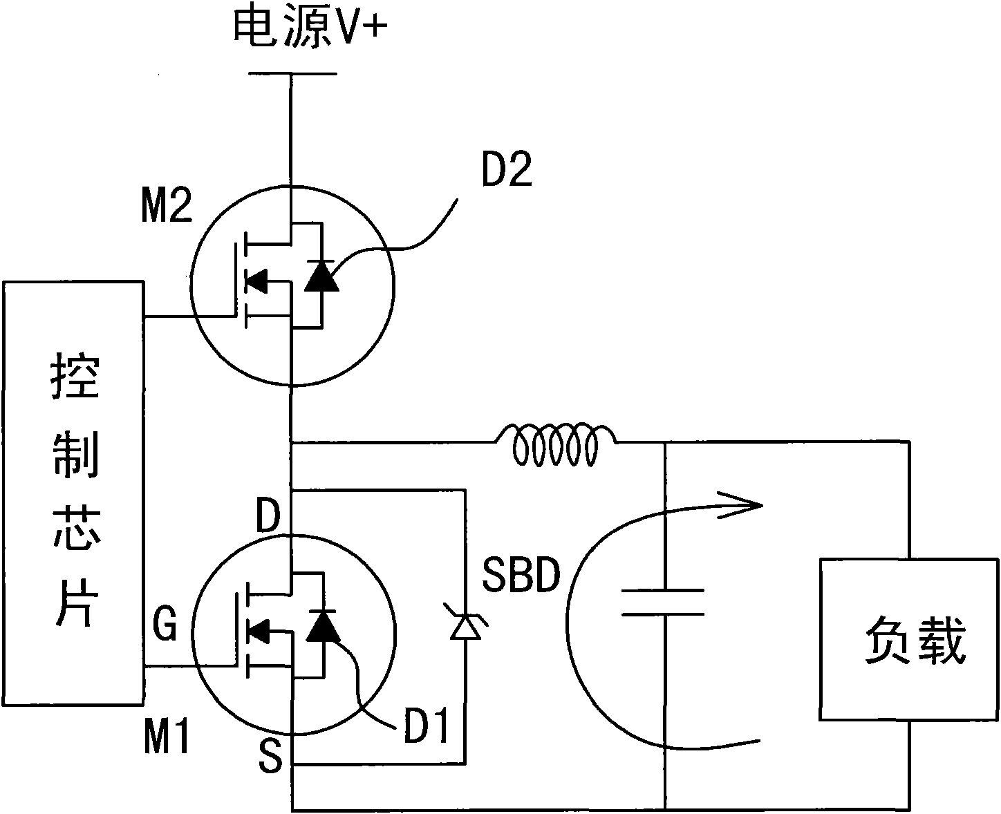
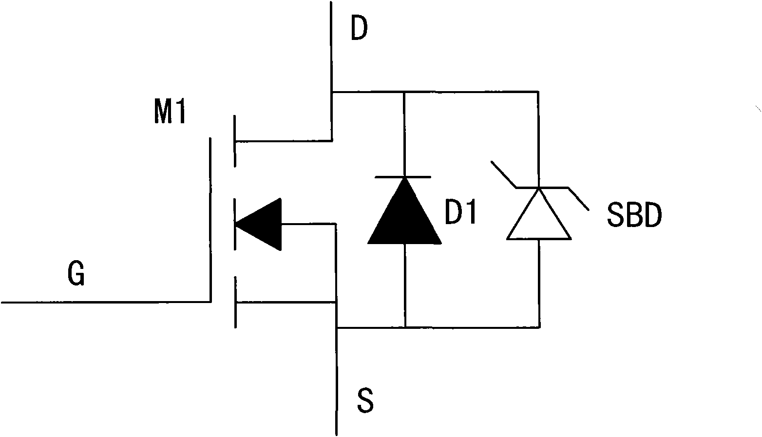
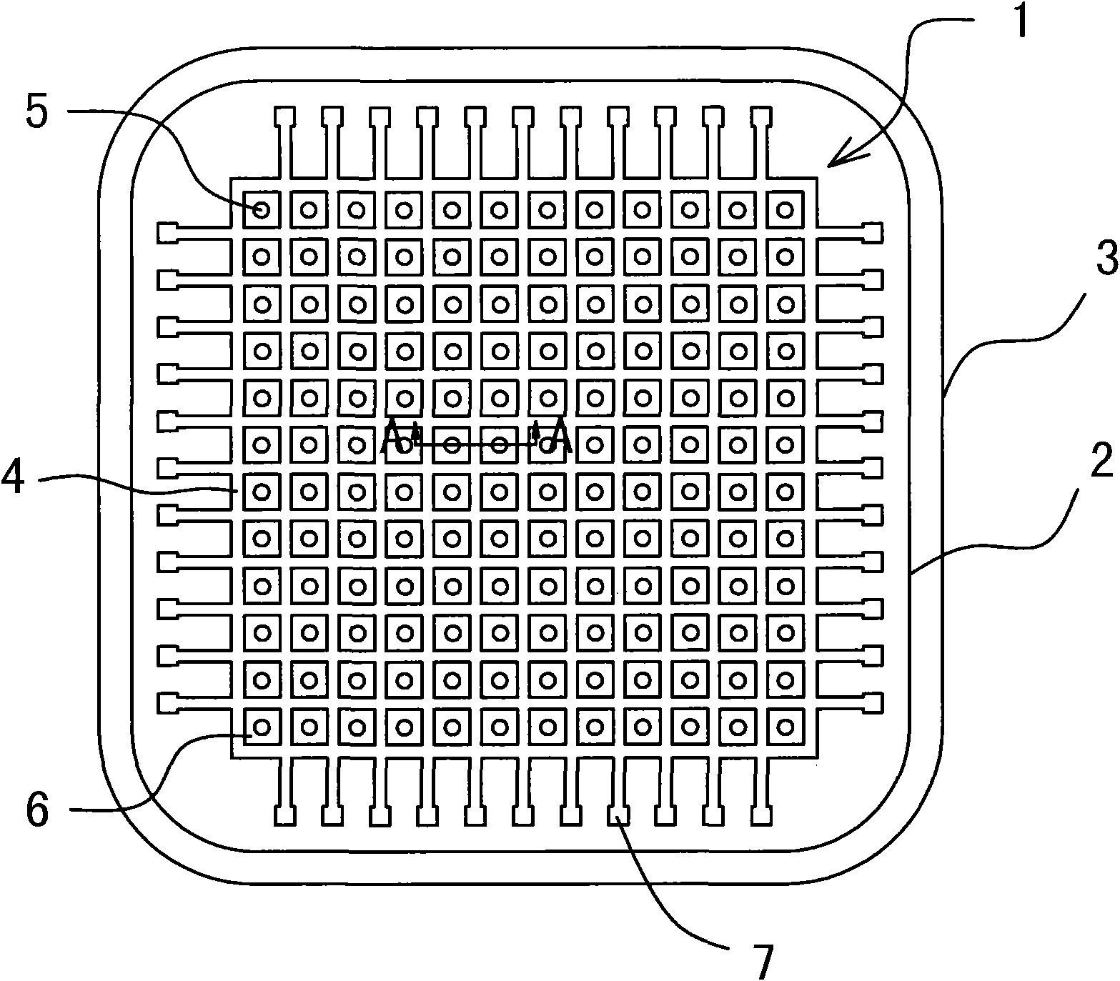
[0059] Such as image 3 and Figure 4 As shown, the structure of the grooved N-type MOS device integrating Schottky diodes in the unit cell of the present invention is: on the top view plane, the center is a parallel unit cell array area 1, and the periphery of the unit cell array area 1 is provided with a guard ring 2 and Stop ring 3 and other terminal protection structures. An upper metal layer 9 is deposited on the top surface of the unit cell array region 1, and the upper metal layer 9 is metal aluminum, or metal aluminum doped with copper, or metal aluminum doped with copper and silicon. The bottom of the unit cell array region 1 includes a lower metal layer (not shown in the figure), an N+ monocrystalline silicon substrate 10 and an N− epitaxial layer 11 from bottom to top. In the N-epitaxial layer 11, several grooves 4 are provided in parallel in the longitudinal direction and the lateral direction, and the several grooves 4 provided in parallel in the longitudinal di...
Embodiment 2
[0096] Such as Figure 6 As shown, the difference between this embodiment and Embodiment 1 is that the gate oxide layer 22 at the bottom of the trench 4 is thicker, that is, the gate oxide layer 22 at the bottom of the trench 4 is thicker than the gate oxide layer on the sidewall of the trench 4 12 thickness, the other structures are basically the same, and will not be described again here. Thickening the gate oxide layer 22 at the bottom of the trench 4 can bring two advantages: first, the parasitic capacitance between the gate and the drain becomes smaller. The switching power loss in the process of dynamic on and off of the MOSFET device can be reduced. Second, when the MOSFET channel is turned off, due to the large bias voltage at the drain, there will be a strong electric field at the bottom of the trench, and a thicker gate oxide layer 22 can improve the ability of the device to withstand strong electric fields and avoid Device failure due to drain-to-gate breakdown. ...
Embodiment 3
[0103] Such as Figure 8 As shown, the difference between this embodiment and Embodiment 1 is that a polysilicon shielding layer 25 is added at the bottom of the trench 4 , and the polysilicon shielding layer 25 is located under the conductive gate polysilicon 13 in the trench 4 . Other structures are basically the same, and will not be described again here. The benefit of adding the polysilicon shielding layer 25 at the bottom of the trench 4 is mainly to reduce the parasitic capacitance between the gate and the drain. The structure can reduce the switching power loss during the dynamic on and off process of the MOSFET device.
[0104] The manufacturing method adopted for adding the polysilicon shielding layer 25 at the bottom of the trench 4 is: based on the process steps of Embodiment 1, the following steps are added between the ninth step and the tenth step:,
[0105] refer to Figure 9A :
[0106] After the ninth step, the upper surface of the whole structure uniforml...
PUM
 Abstract
Description
Claims
Application Information
 - R&D
- Intellectual Property
- Life Sciences
- Materials
- Tech Scout
- Unparalleled Data Quality
- Higher Quality Content
- 60% Fewer Hallucinations
Browse by: Latest US Patents, China's latest patents, Technical Efficacy Thesaurus, Application Domain, Technology Topic, Popular Technical Reports.
© 2025 PatSnap. All rights reserved.Legal|Privacy policy|Modern Slavery Act Transparency Statement|Sitemap|About US| Contact US: help@patsnap.com