Single-electron magnetic resistance structure and application thereof

A single-electron, tunneling magneto-resistance technology, which is applied in the fields of magnetic storage and spintronics, can solve problems such as inadaptability, low signal-to-noise ratio, and high power consumption, so as to reduce power consumption, improve signal-to-noise ratio, and improve The effect of the tunneling magnetoresistance effect

Active Publication Date: 2010-10-06
INST OF PHYSICS - CHINESE ACAD OF SCI
View PDF0 Cites 11 Cited by
  • Summary
  • Abstract
  • Description
  • Claims
  • Application Information

AI Technical Summary

Problems solved by technology

However, the signal-to-noise ratio and high power consumption of these two types of magnetoresistance structures at the scale of 100 nanometers are still relatively low, which cannot meet the requirements of further development of higher density and miniaturized spintronics devices in the future.

Method used


Image

  • Single-electron magnetic resistance structure and application thereof
  • Single-electron magnetic resistance structure and application thereof
  • Single-electron magnetic resistance structure and application thereof

Examples


Embodiment 1

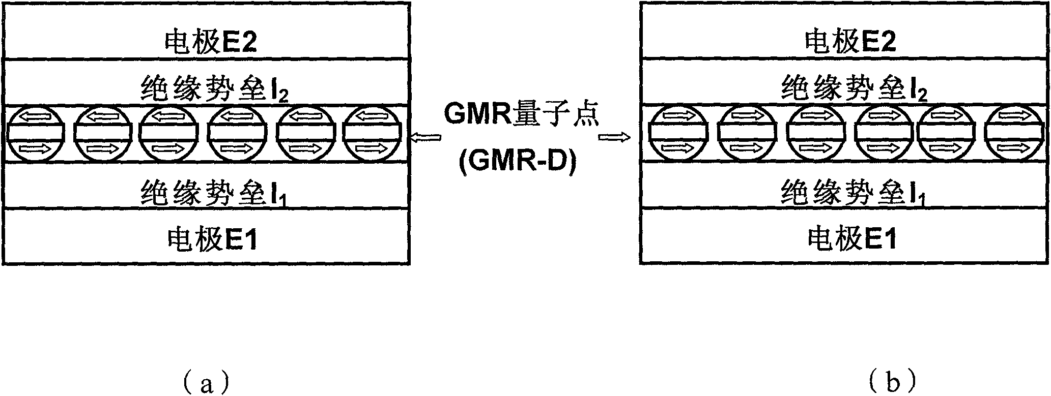
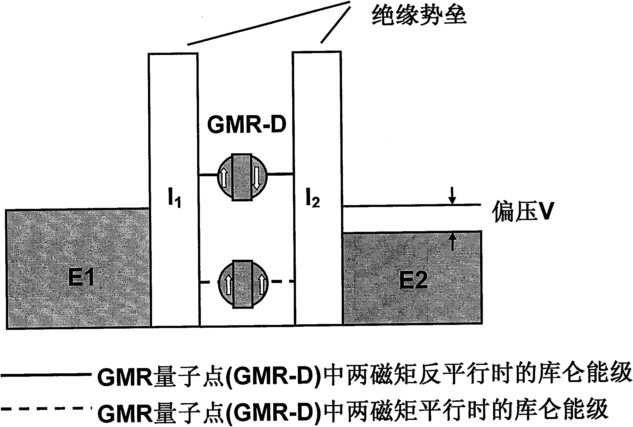
[0039] According to an embodiment of the present invention, a GMR quantum dot single-electron tunneling magnetoresistance structure is provided. Such as figure 1 (a) and figure 1 As shown in (b), it is a schematic diagram of the longitudinal cross-sectional structure of the GMR quantum dot single-electron tunneling magnetoresistance structure of the embodiment of the present invention under the conditions of antiparallel and parallel magnetic moments of the GMR quantum dot, respectively. The GMR quantum dot single-electron tunneling magnetoresistance structure includes a substrate (not shown), and an electrode E1 (also called a bottom conductive layer), a core film layer, and an electrode E2 (also called a top conductive layer) thereon, wherein The core film layer includes from bottom to top: an insulating barrier layer I1, a GMR magnetic quantum dot layer GMR-D (ie, GMR Dots), an insulating barrier layer I2, that is, the structure of the core film layer can be expressed as I...

Embodiment 2

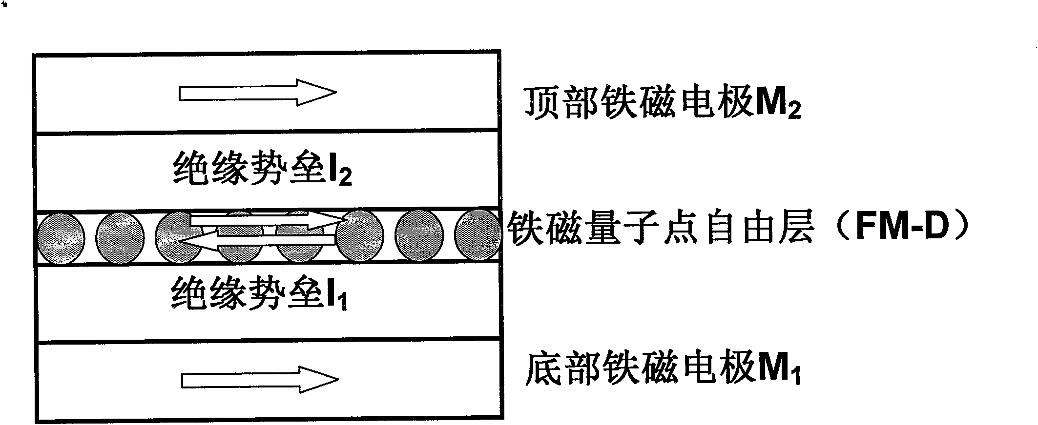
[0050] According to another embodiment of the present invention, a double-barrier magnetic quantum dot magnetoresistance structure using magnetic materials as electrodes is provided. The double potential barrier magnetic quantum dot structure includes a substrate, a lower buffer conductive layer, a lower antiferromagnetic pinning layer, a core film layer, an upper antiferromagnetic pinning layer, a top protection layer and a conductive layer. Figure 5 It is a schematic cross-sectional structure diagram of the core film layer of the magnetic electrode double barrier quantum dot structure of the present invention. The core membrane layer such as Figure 5 Shown from bottom to top includes: bottom ferromagnetic electrode M1, insulating barrier layer I1, ferromagnetic quantum dot layer FM-D (Ferromagnetic-Dots), insulating barrier layer I2 and top ferromagnetic electrode M2, that is, the core film layer The structure can be expressed as M1 / I1 / FM-D / I2 / M2. The FM-D layer includes...

Embodiment 3

[0065] [Example 3]: spin diode based on the GMR quantum dot single electron tunneling magnetoresistance structure or double barrier magnetic quantum dot structure of the present invention

[0066] The GMR quantum dot single-electron tunneling magnetoresistance structure and the double potential barrier magnetic quantum dot structure of the present invention can be used in a spin diode. Common diodes are composed of p-n junction connections and have unidirectional conduction characteristics of current. The single-electron magnetoresistive structure based on Coulomb blockade proposed by the present invention can only be conducted in a positive bias (or negative bias) unidirectionally due to the different positions of the spin-related energy levels, and has a larger conductive channel, thereby It has a large current and does not conduct under reverse bias, so it can be used as a spin diode. Due to the adoption of the single-electron tunneling magnetoresistance structure of the p...


PUM


Abstract

The invention discloses a single-electron magnetic resistance structure and application thereof, such as a spin diode, a spin transistor, a sensor, a magnetic random access memory and a magnetic logic device unit. A GMR (Giant Magnetic Resistance) quantum dot single-electron tunneling magnetic resistance structure comprises a substrate as well as a bottom conducting layer, a first barrier layer, a GMR magnetic quantum dot layer, a second barrier layer and a top conducting layer which are arranged on the substrate. A double-barrier magnetic quantum dot structure comprises a core film layer comprising a bottom electrode, a first barrier layer, a magnetic quantum dot layer, a second barrier layer and a top electrode from bottom to top. Due to the combination with a coulomb blockade effect and a tunneling magnetic resistance effect, the invention controls coulomb energy level resonant tunneling passing through quantum dots by utilizing an external magnetic field to improve tunneling magnetic resistance. The invention can effectively improve the tunneling magnetic resistance effect by utilizing a magnetic resistance design formed by coulomb blockade and improve the signal to noise ratio of device application, and simultaneously reduces tunneling current by utilizing single-electron tunneling, thereby reducing the power consumption of device application.

Description

technical field [0001] The invention relates to the fields of magnetic storage and spin electronics, in particular to a single-electron magnetoresistance structure and its spin diode, spin transistor, sensor, magnetic random access memory and magnetic logic device unit. Background technique [0002] The usual magnetoresistance structure is composed of a ferromagnetic / nonmagnetic / ferromagnetic layered sandwich structure. When the magnetization directions of the two magnetic electrodes are parallel and antiparallel, the resistance will change, which is called the magnetoresistance effect. When the middle non-magnetic layer is non-magnetic metal or insulating barrier, it corresponds to Giant Magnetoresistance-GMR and Tunneling Magnetoresistance-TMR structures, such as Co / Cu / Co and CoFeB / AlOx / CoFeB. However, the signal-to-noise ratio and high power consumption of these two types of magnetoresistive structures at the scale of 100 nanometers are still relatively low, which cannot ...

Claims


Application Information

Patent Timeline
Patent Type & Authority Applications(China)
IPC IPC(8): H01L43/08H01L29/66H01L27/22H01L43/12G11C11/15G01R33/09
CPCG11C11/161
Inventor 张佳温振超张晓光韩秀峰
Owner INST OF PHYSICS - CHINESE ACAD OF SCI
Why Eureka
Try Eureka