Silicon chip phosphorous diffusion impurity removal process for manufacturing solar cell
A technology of solar cells and phosphorus diffusion, applied in the directions of diffusion/doping, crystal growth, post-processing, etc., can solve the problem that metal impurities cannot be effectively reduced, and achieve the effect of improving light conversion efficiency and reducing content
- Summary
- Abstract
- Description
- Claims
- Application Information
AI Technical Summary
Problems solved by technology
Method used
Image

Examples
Embodiment 1
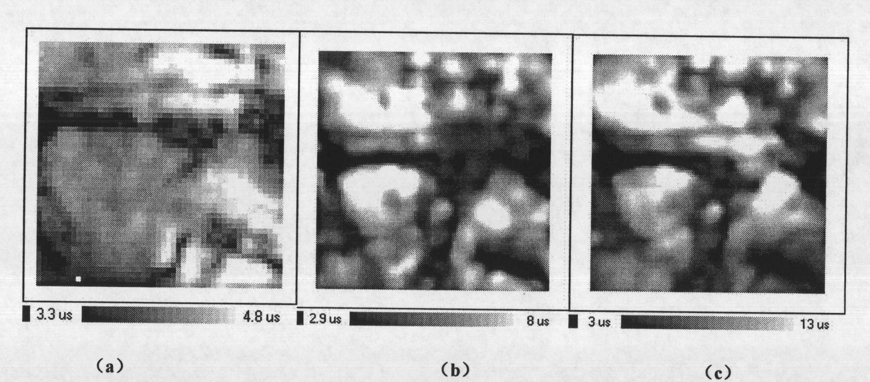
[0028] (1) Take the original cast polysilicon wafer, such as figure 2 As shown in (a), the minority carrier lifetime is about 4 μs after testing;
[0029] (2) Spin-coat both sides of the above-mentioned silicon wafer with a phosphorus source (p-854, Honeywell), and then pre-bake at 200°C for 10 minutes to remove organic matter;
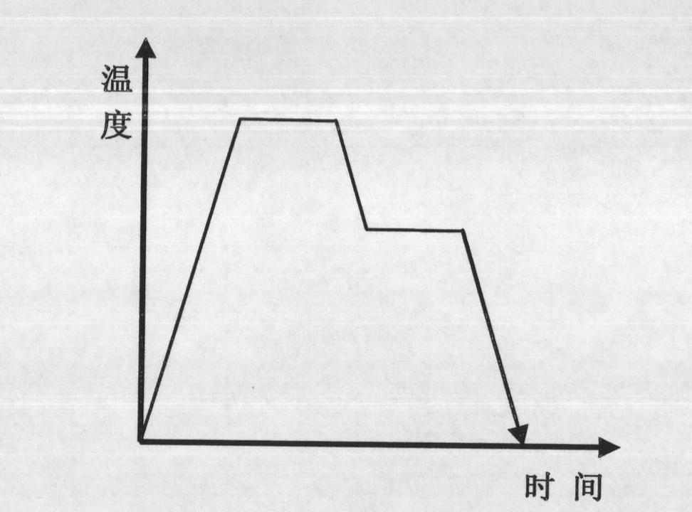
[0030] (3) Pass the protective gas (argon) into the diffusion furnace. The diffusion furnace does not need to be closed, and the air pressure is about 1 atmosphere. Place the baked silicon wafer in the diffusion furnace, and control the temperature in the furnace to 1000°C , keep warm for 30min; then control the temperature in the furnace to 700°C, keep warm for 60min, and take the same treated silicon wafer and place it in a diffusion furnace with a furnace temperature of 900°C for 60min, as a control group;
[0031] (4) Take out the silicon chip, after cooling, remove the phosphosilicate glass layer with dilute HF (volume concentration 10%);
[0...
Embodiment 2
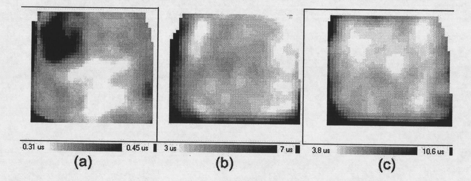
[0034] (1) Take the original single crystal silicon wafer, the minority carrier lifetime is about 6μs after detection, after iron contamination, the minority carrier lifetime drops to 0.4μs, as image 3 as shown in (a);
[0035] (2) Spin-coat both sides of the above-mentioned monocrystalline silicon wafer with a phosphorus source (p-854, Honeywell), and then pre-bake at 200°C for 10 minutes to remove organic matter;
[0036] (3) Pass the protective gas (argon gas) into the diffusion furnace. The diffusion furnace does not need to be closed. 850°C, keep warm for 30 minutes, then control the temperature in the furnace to 700°C, keep warm for 90 minutes, and take the same treated monocrystalline silicon wafers and place them in a diffusion furnace with a furnace temperature of 900°C for 120 minutes, as a control group;
[0037] (4) Take out the silicon chip, after cooling, remove the phosphosilicate glass layer with dilute HF (volume concentration 10%);
[0038] Such as image...
Embodiment 3
[0040] (1) Take native polysilicon wafers, such as Figure 4 As shown in (a), the minority carrier lifetime is about 3.5 μs after detection. After iron contamination, as Figure 4 As shown in (b), the minority carrier lifetime drops to 0.3μs;
[0041] (2) Spin-coat both sides of the above-mentioned polysilicon wafer with a phosphorus source (p-854, Honeywell), and then pre-bake at 200° C. for 10 minutes;
[0042] (3) Pass the protective gas (argon gas) into the diffusion furnace. The diffusion furnace does not need to be closed. 900°C, heat preservation for 10 minutes, then control the temperature in the furnace to 650°C, heat preservation for 50 minutes, and at the same time take the same treated monocrystalline silicon wafer and place it in a diffusion furnace with a furnace temperature of 900°C for 60 minutes, as a control group;
[0043] (4) Take out the silicon chip, after cooling, remove the phosphosilicate glass layer with dilute HF (volume concentration 10%);
[004...
PUM
| Property | Measurement | Unit |
|---|---|---|
| Life expectancy | aaaaa | aaaaa |
| Life expectancy | aaaaa | aaaaa |
Abstract
Description
Claims
Application Information
 - Generate Ideas
- Intellectual Property
- Life Sciences
- Materials
- Tech Scout
- Unparalleled Data Quality
- Higher Quality Content
- 60% Fewer Hallucinations
Browse by: Latest US Patents, China's latest patents, Technical Efficacy Thesaurus, Application Domain, Technology Topic, Popular Technical Reports.
© 2025 PatSnap. All rights reserved.Legal|Privacy policy|Modern Slavery Act Transparency Statement|Sitemap|About US| Contact US: help@patsnap.com