Surface plasma resonance sensor chip and preparation method thereof

A surface plasmon and resonance sensor technology, applied in the direction of ion implantation plating, coating, metal material coating process, etc., can solve the problems of cumbersome operation, poor selectivity, low sensitivity, etc., and achieve simple operation steps and controllable thickness Effect

Inactive Publication Date: 2010-11-17
BEIJING INSTITUTE OF TECHNOLOGYGY
View PDF4 Cites 30 Cited by
  • Summary
  • Abstract
  • Description
  • Claims
  • Application Information

AI Technical Summary

Problems solved by technology

[0020] The purpose of the present invention is to solve the problems of low sensitivity and cumbersome operation in the preparation of surface plasmon resonance chips by using molecular imprinting technology in the prior art, and propose a surface plasmon resonance sensor chip and its preparation method, which effectively solves the problem of using molecular imprinting technology. It is difficult to control the thickness of the molecularly imprinted film, poor selectivity and low sensitivity when preparing surface plasmon resonance chips. At the same time, the preparation method has fewer steps and lower production costs, which is more suitable for industrial production

Method used


Image

  • Surface plasma resonance sensor chip and preparation method thereof
  • Surface plasma resonance sensor chip and preparation method thereof
  • Surface plasma resonance sensor chip and preparation method thereof

Examples


Embodiment 1

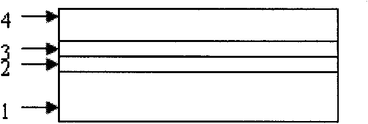
[0043] A surface plasmon resonance sensor chip, such as figure 1 As shown, it includes a glass substrate 1, a gold film layer 2, a monomolecular alkyl chain layer 3 and a molecularly imprinted polymer film 4; Base chain layer 3 and molecularly imprinted polymer film 4;

[0044] The structural formula of the monomolecular alkyl chain layer 3 is Au-(CH 2 ) 11 CH 3 ;

[0045] The molecularly imprinted polymer film 4 is obtained by photopolymerization of template molecules, functional monomers, crosslinking agents, pore forming agents and photoinitiators, the template molecule is the target molecule testosterone to be imprinted, and the functional monomer is methacrylic acid The crosslinking agent is ethylene glycol dimethacrylate; the pore forming agent is acetonitrile;

[0046] A method for preparing a surface plasmon resonance sensor chip, the specific steps of which are:

[0047] 1) The method of vacuum evaporation is used to plate a gold film layer 2 on the glass substr...

Embodiment 2

[0057] A surface plasmon resonance sensor chip, such as figure 1 As shown, it includes a glass substrate 1, a gold film layer 2, a monomolecular alkyl chain layer 3 and a molecularly imprinted polymer film 4; Base chain layer 3 and molecularly imprinted polymer film 4;

[0058]The structural formula of the monomolecular alkyl chain layer 3 is Au-(CH 2 ) 11 CH 3 ;

[0059] The molecularly imprinted polymer film 4 is obtained by photopolymerization of template molecules, functional monomers, crosslinking agents, pore forming agents and photoinitiators, the template molecule is the target molecule testosterone to be imprinted, and the functional monomer is methacrylic acid The crosslinking agent is ethylene glycol dimethacrylate; the pore forming agent is acetonitrile;

[0060] A method for preparing a surface plasmon resonance sensor chip, the specific steps of which are:

[0061] 1) with 1) in embodiment 1;

[0062] 2) with 2) in embodiment 1;

[0063] 3) with 3) in emb...


PUM


Abstract

The invention relates to a surface plasma resonance sensor chip and a preparation method thereof, in particular to a photografting molecularly imprinted polymer membrane-based surface plasma resonance sensor chip and a preparation method thereof, and belongs to the field of surface plasma sensor chip preparation. The chip comprises a glass substrate, a gold membrane layer, a unimolecular alkyl chain layer and a molecular imprinted polymer membrane, wherein the gold membrane layer is plated on the glass substrate, the unimolecular alkyl chain layer is self-assembled on the glass substrate, and the molecular imprinted polymer membrane is grafted on the unimolecular alkyl chain layer in turn. The molecular imprinted membrane with nanoscale thickness can be conveniently and quickly prepared on the surface of the gold membrane by the preparation method and has controllable thickness; the growth changes of the molecular imprinted membrane can be dynamically monitored in real time in situ; operation steps are simple and deoxidation and nitrogen protection are not needed; and the matrix type molecular imprinted structural units are easy to prepare on the surface of the gold membrane, each unit can be different template molecules and multi-channel and multi-target molecular detection is realized.

Description

technical field [0001] The invention relates to a surface plasmon resonance (Surface Plasmon Resonance, referred to as SPR) sensor chip and a preparation method thereof, in particular to a surface plasmon resonance sensor chip based on a photografted molecularly imprinted polymer film and a preparation method thereof, belonging to Surface plasmon sensor chip preparation field. Background technique [0002] SPR sensors use incident light to excite surface plasmon waves (Surface Plasmon Wave, or SPW) on the interface between metal and dielectric through a certain coupling method to realize information conversion. Taking the prism coupling structure as an example, when the incident light propagates from the optically denser medium to the optically rarer medium and the incident angle is in an appropriate range, total internal reflection will occur at the interface of the two substances. If the component of the wave vector of the incident light along the parallel interface is eq...

Claims


Application Information

Patent Timeline
Patent Type & Authority Applications(China)
IPC IPC(8): G01N21/41C23C14/24C23C14/34C23C14/18
Inventor 魏清泉韦天新张庆文
Owner BEIJING INSTITUTE OF TECHNOLOGYGY
Why Eureka
Try Eureka