Wafer-level integrated encapsulation method of MEMS (Micro Electric Mechanical System) devices requiring different atmosphere pressures

An integrated packaging, wafer-level technology, used in instruments, decorative arts, gaseous chemical plating, etc., can solve the problem of different quality factor requirements of movable parts, and achieve increased quality factor, convenient operation and simple method. Effect

Active Publication Date: 2010-12-01
SOUTHEAST UNIV
View PDF4 Cites 21 Cited by
  • Summary
  • Abstract
  • Description
  • Claims
  • Application Information

AI Technical Summary

Problems solved by technology

Although many different types of MEMS devices are compatible in terms of technology, because different MEMS

Method used


Image

  • Wafer-level integrated encapsulation method of MEMS (Micro Electric Mechanical System) devices requiring different atmosphere pressures
  • Wafer-level integrated encapsulation method of MEMS (Micro Electric Mechanical System) devices requiring different atmosphere pressures
  • Wafer-level integrated encapsulation method of MEMS (Micro Electric Mechanical System) devices requiring different atmosphere pressures

Examples


Embodiment 1

[0030] Embodiment 1 The method of utilizing glass microcavity to carry out wafer-level hermetic packaging

[0031] A MEMS device wafer-level integrated packaging method requiring different atmosphere pressures, comprising the following steps:

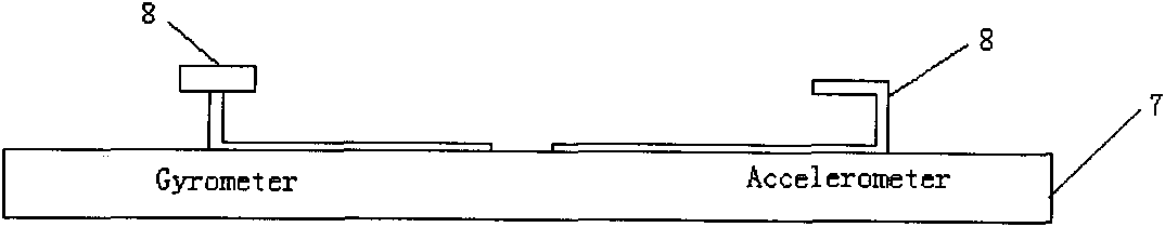
[0032] The first step is to manufacture at least two MEMS devices requiring different quality factors, such as MEMS accelerometers and gyroscopes, on silicon wafers using conventional MEMS processing technology. The specific process can be silicon surface technology or bulk microtechnology. The thickness of the insulating layer (silicon dioxide) is 0.1-0.5 microns, such as the integrated piezoresistive accelerometer and gyroscope of Maxic or AD Company, the leads can be set at the same time, and the lead-out method of the lead cavity can be used to realize the lead-out of the chip.

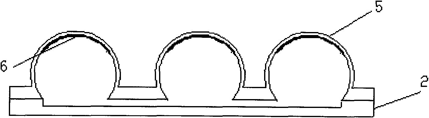
[0033] In the second step, a glass wafer with a glass microcavity sealing the MEMS chip is prepared by thermoforming at a position corresponding to the abo...

Embodiment 2

[0037] Embodiment 2 The method of utilizing glass microcavity to carry out wafer-level hermetic packaging

[0038] A MEMS device wafer-level integrated packaging method requiring different atmosphere pressures, comprising the following steps:

[0039] The first step is to prepare comb-teeth MEMS accelerometers and gyroscopes (commercially achievable) on the same silicon wafer using standard CMOS technology. Aluminum leads are made on the surface of the silicon wafer with a thickness of 0.3 microns and an insulating layer with a thickness of 0.3 microns. .

[0040] In the second step, a glass wafer with a glass microcavity sealing the MEMS chip is prepared by thermoforming at a position corresponding to the above-mentioned MEMS device on the glass wafer, and a getter is deposited in the glass microcavity encapsulating the MEMS chip to obtain a functionalized For the glass wafer, the method for preparing the glass microcavity is shown in Example 4 of the present invention. At ...

Embodiment 3

[0043] The positive pressure preparation method of embodiment 3 glass microcavities

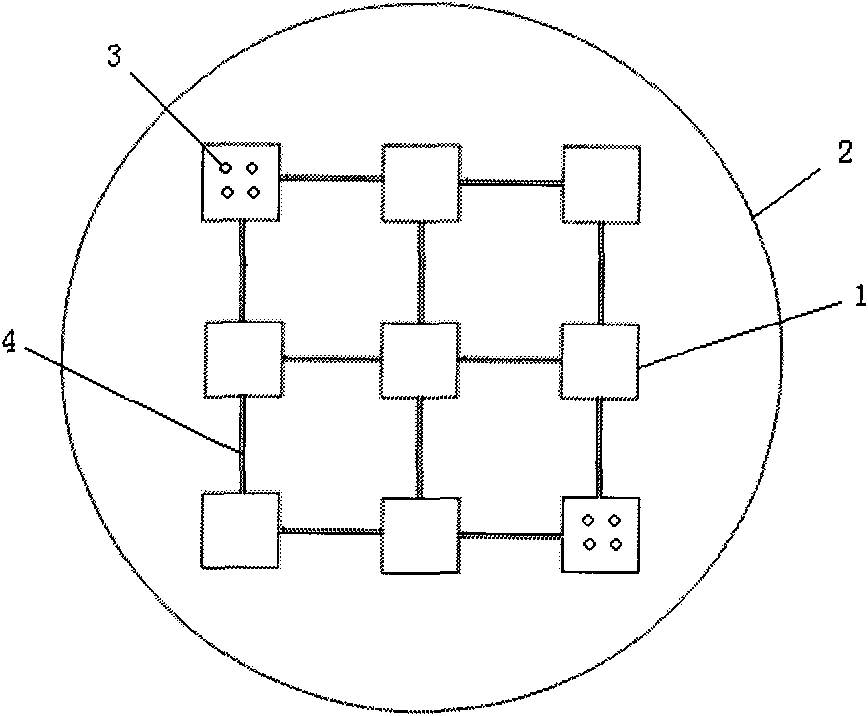
[0044]A MEMS device wafer-level integrated packaging method requiring different atmosphere pressures, comprising the following steps: the silicon wafer is engraved with an array formed by the same microgrooves (the size of the microgrooves is the same), and the method of etching the microgrooves can be a dry method And wet method, preferably wet method (the required microgroove depth of the present invention can place heat release agent, so adopting wet etching shallower depth just can meet the requirements, such as the depth of 50-100 microns), so The etched microgrooves have the same size (for example, 5, 10, 15, 50), microchannels are carved between the microgrooves, and the minimum groove width of the microgrooves is greater than 5 times the width of the flow channel. Place an appropriate amount of heat release agent in at least one microgroove (can place heat release agent in two or more...


PUM

PropertyMeasurementUnit
Thicknessaaaaaaaaaa
Depthaaaaaaaaaa
Thicknessaaaaaaaaaa

Abstract

The invention discloses a wafer-level integrated encapsulation method of MEMS (Micro Electric Mechanical System) devices requiring different atmosphere pressures. The method comprises the following steps of: 1. preparing at least two MEMS devices requiring different quality factors on a silicon wafer; 2. preparing a glass micro-cavity for sealing an MEMS chip corresponding to the positions of the MEMS devices on a glass wafer with a thermoforming method, and depositing a getter in the glass micro-cavity in which the MEMS chip is encapsulated to obtain a functionalized glass wafer; 3. carrying out anodic bonding on the functionalized glass wafer and the silicon wafer with the MEMS devices so as to hermetically encapsulating the MEMS devices; and 4. selectively heating the getter in the glass micro-cavity in which the MEMS chip is encapsulated by laser to absorb air so that the quality factor in the cavity is changed. In the method, the getter is arranged in each cavity, and the quality factor in the encapsulation cavity is changed selectively by heating and activating.

Description

technical field [0001] The invention relates to a MEMS (micro-electro-mechanical system) manufacturing technology, in particular to a wafer-level integrated packaging method for MEMS devices requiring different atmosphere pressures. Background technique [0002] In the field of MEMS packaging, since devices generally contain movable parts, it is necessary to use a micron-sized microcavity structure to hermetically package the device during packaging, so that the movable parts have room for movement and provide physical protection for the device. Some such as Devices such as resonators, gyroscopes, and accelerometers also require a vacuum-tight packaging environment. At present, our commonly used bonding packaging processes include silicon-glass anodic bonding, silicon-silicon thermal bonding, fused glass sealing and organic adhesive bonding. Among them, the temperature of silicon-silicon thermal bonding is too high and the time is long, and the process is difficult to grasp...

Claims


Application Information

Patent Timeline
IPC IPC(8): B81C1/00B81C3/00
Inventor 尚金堂张迪徐超陈波寅
Owner SOUTHEAST UNIV
Why Eureka
Try Eureka