

GaN-based light emitting diode and preparation method thereof
A light-emitting diode, gallium nitride-based technology, applied in the direction of electrical components, circuits, semiconductor devices, etc., can solve the problems of total reflection loss of light emission, limitation of light emission efficiency, etc., to reduce the impact, enhance the light output efficiency, and improve the electro-optic conversion efficiency. Effect
- Summary
- Abstract
- Description
- Claims
- Application Information
AI Technical Summary
Problems solved by technology
Method used
Image


Examples
Embodiment 1
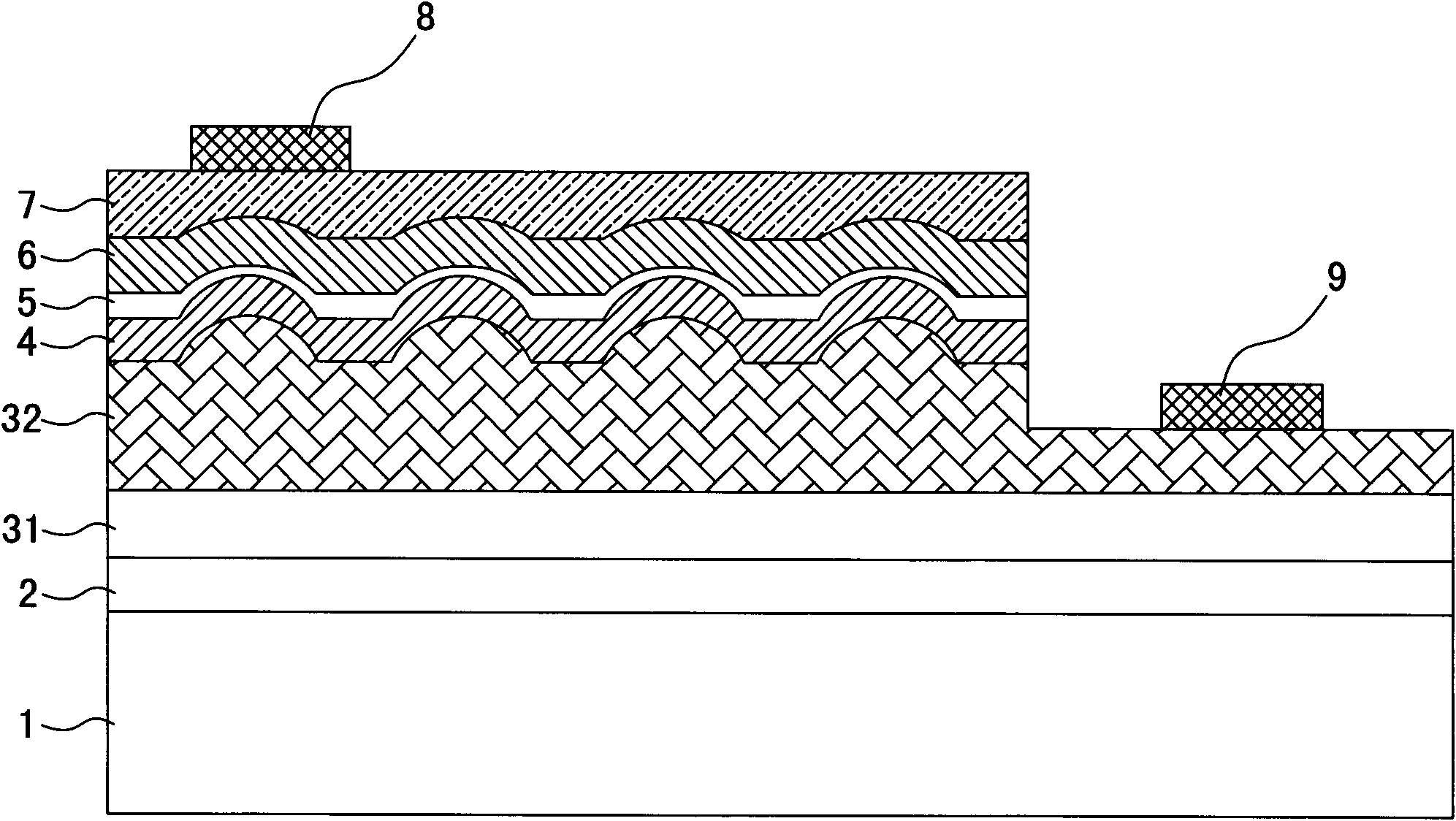
[0043] see figure 1 Shown, a gallium nitride-based light-emitting diode, its preparation method comprises the following steps:
[0044] (1) On a substrate 1 such as a planar sapphire substrate, a patterned sapphire substrate, a gallium nitride substrate, a silicon carbide substrate or a silicon substrate, a buffer layer 2 and an intrinsic GaN layer 31 and N-type doped GaN are grown The epitaxial layer 32; the total thickness of the intrinsic GaN layer and the N-type doped GaN epitaxial layer is 3-7 μm, depending on the substrate type;
[0045] (2) Prepare an N-type GaN patterned template structure on the N-type doped GaN epitaxial layer by reactive ion etching, holographic exposure method or electron beam exposure method; the N-type GaN patterned template structure is a continuous yurt shape, The diameter, height, and distance between adjacent yurts are matched to each other, and its magnitude extends from nanometers to micrometers;
[0046] (3) Epitaxial In on the N-type Ga...
PUM
| Property | Measurement | Unit |
|---|---|---|
| Thickness | aaaaa | aaaaa |
| Thickness | aaaaa | aaaaa |
| Thickness | aaaaa | aaaaa |
Abstract
Description
Claims
Application Information