Unlock instant, AI-driven research and patent intelligence for your innovation.
Semiconductor substrate and preparation method thereof
What is Al technical title?
Al technical title is built by PatSnap Al team. It summarizes the technical point description of the patent document.
A semiconductor and substrate technology, applied in the field of semiconductor substrates and their preparation, can solve the problems of easy cracking, volatility and corrosion of GaN
Inactive Publication Date: 2011-01-26
SHANGHAI RES CENT OF ENG & TECH FOR SOLID STATE LIGHTING
View PDF0 Cites 4 Cited by
Summary
Abstract
Description
Claims
Application Information
AI Technical Summary
This helps you quickly interpret patents by identifying the three key elements:
Problems solved by technology
Method used
Benefits of technology
Problems solved by technology
[0007] The technical problem to be solved by the present invention is to provide a preparation method capable of preparing a semiconductor substrate, through which the lithium aluminate substrate is improved to overcome the corrosion-prone, Li Volatility, and the problem of easy cracking of GaN due to the difference in thermal expansion coefficient between lithium aluminate and GaN
Method used
Image
Click on the blue label to locate the original text in one second.
Reading with bidirectional positioning of images and text.
Examples
Embodiment approach
[0026] An embodiment of preparing a semiconductor substrate of the present invention includes:
[0027] Provide lithium aluminate wafer;
[0028] A semiconductor substrate is obtained by depositing an AlN film layer on the lithium aluminate wafer by using a sputtering method.
[0029] According to the present invention, the lithium aluminate wafer is used as the base of the semiconductor substrate, and the lithium aluminate wafer needs to be polished. For the surface roughness of the lithium aluminate wafer, the root mean square roughness is preferably less than 10 angstroms, more preferably less than 8 angstroms , more preferably less than 5 angstroms. For the polishing method of the lithium aluminate wafer, the present invention is not particularly limited. According to the present invention, a (100) crystal plane lithium aluminate wafer is preferred as the base material of the semiconductor substrate.
[0030] According to the present invention, a sputtering method is us...
Embodiment 1
[0038] Place the polished lithium aluminate wafer with a surface root mean square roughness of 5 Angstroms (100) in the sputtering chamber of the measurement and control sputtering system, and vacuum the sputtering chamber to 2.0×10 -4 Pa; heat the lithium aluminate wafer to 400 °C and keep it warm, with flowing Ar and N 2 As sputtering gas, the flow rate of sputtering gas is about 15 sccm, Ar and N 2 The volume ratio is 3:1.
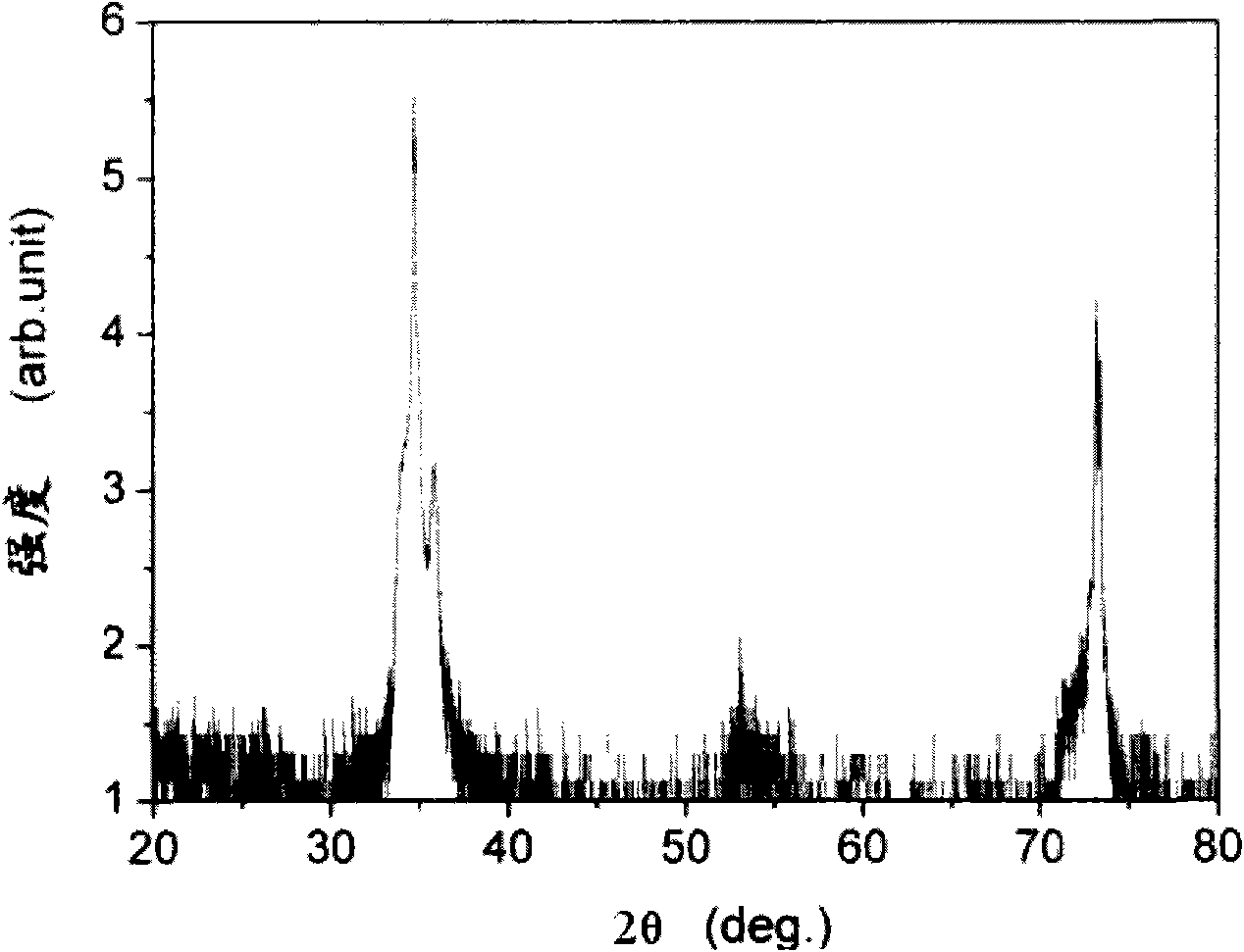
[0039] Using AlN ceramics with a purity of 99.99wt% as the target material, using radio frequency sputtering, the sputtering power is 200W, and the sputtering time is 20 minutes. After the sputtering, the lithium aluminate wafer deposited with AlN is cooled to Remove from room temperature. Carry out XRD test on the semiconductor substrate, the test results are as follows figure 1 As shown, the diffraction peaks located at 34.70°, 35.86°, and 73.19° in the figure correspond to the (200) crystal plane of lithium aluminate, the (0002) crystal plane of A...
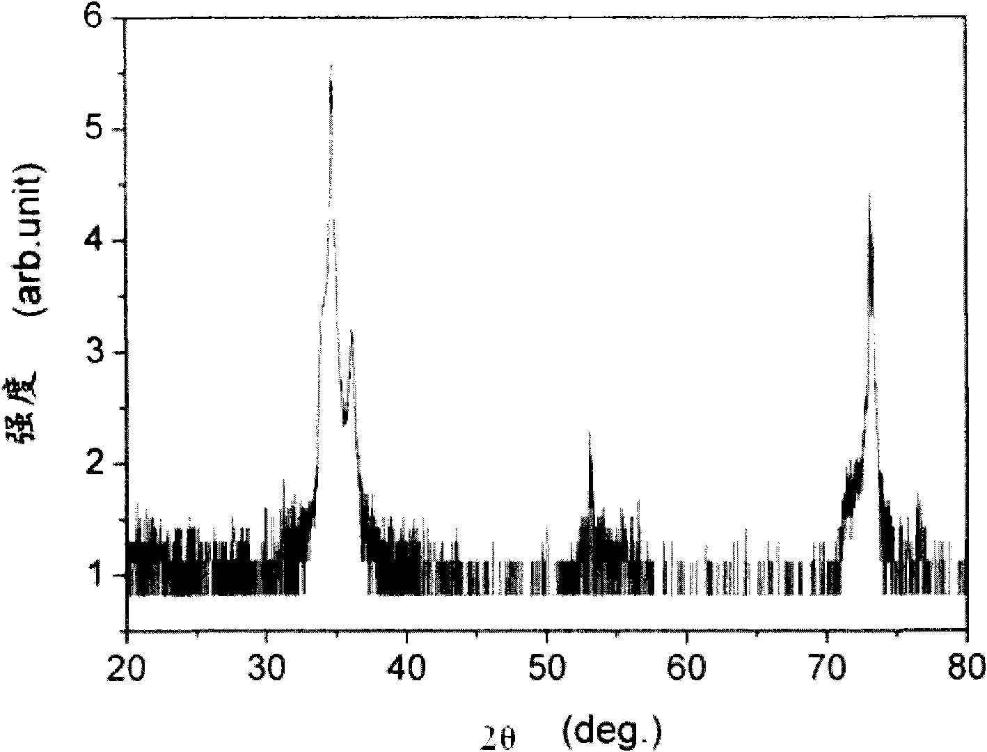
Embodiment 2-4
[0041] In these three embodiments, the RF sputtering power in Embodiment 1 was adjusted to 300W, 400W, and 500W, and the sputtering time was 20 minutes, 30 minutes, and 40 minutes, respectively, and the others were the same as in Embodiment 1.
[0042] The three examples also produced (0001) aluminum nitride films with a high c-axis preferred orientation on the (100) plane lithium aluminate wafer.
technical field [0001] The invention relates to the field of semiconductors, in particular to a semiconductor substrate and a preparation method thereof. Background technique [0002] Group III-IV nitrides (InN, GaN, AlN) represented by GaN and their ternary and quaternary alloys have wide band gap, high electron drift saturation velocity, high thermal conductivity, high breakdown field strength, and high temperature resistance. It is an important direct band gap semiconductor material with excellent physical and chemical properties such as acid and alkali corrosion resistance, and has great application potential in blue light-emitting diodes, laser diodes, short-wavelengthphotodetection devices, and high-frequency high-power electronic devices. [0003] However, it is very difficult to grow GaN single crystals. At present, the growth of GaN thin films is mainly based on c-plane sapphire substrates, or using hydrogenated epitaxy (HVPE) to grow GaN self-supporting substrates...
Claims
Application Information
Patent Timeline
Application Date:The date an application was filed.
Publication Date:The date a patent or application was officially published.
First Publication Date:The earliest publication date of a patent with the same application number.
Issue Date:Publication date of the patent grant document.
PCT Entry Date:The Entry date of PCT National Phase.
Estimated Expiry Date:The statutory expiry date of a patent right according to the Patent Law, and it is the longest term of protection that the patent right can achieve without the termination of the patent right due to other reasons(Term extension factor has been taken into account ).
Invalid Date:Actual expiry date is based on effective date or publication date of legal transaction data of invalid patent.
IPC IPC(8): H01L21/02H01L21/203C23C14/34C23C14/06
Inventor 杨卫桥王康平周颖圆马可军李抒智钱雯磊
Owner SHANGHAI RES CENT OF ENG & TECH FOR SOLID STATE LIGHTING

