
Method for realizing graded laminated passivation film on back surface of solar cell

A technology of solar cells and passivation films, applied in coatings, circuits, photovoltaic power generation, etc., can solve problems such as side effects of SiNx, drop in output current and voltage, and reduced life of polycrystals, achieve superior back passivation, reduce compliance rate, the effect of reducing film stress

Inactive Publication Date: 2011-02-02
TRINA SOLAR CO LTD
View PDF2 Cites 18 Cited by
  • Summary
  • Abstract
  • Description
  • Claims
  • Application Information

AI Technical Summary

Problems solved by technology

At present, the existing back surface passivation methods are: 1. Aluminum back field passivation. At present, most crystalline silicon solar cells use the method of screen printing aluminum back field, but the passivation effect is limited; 2. Thermal growth oxidation Silicon passivation, the passivation effect of thermally grown silicon dioxide passivation is good, but it has a disadvantage. The cell has to go through the process of thermally growing silicon oxide at high temperature. The high temperature is usually greater than 800 degrees. There are side effects, and it will reduce the life of the polycrystal, and the process time will be longer; 3. SiNx passivation has a good passivation, but this inversion layer will introduce a field, which will form a bypass to greatly reduce the output current and voltage

Method used


Image

  • Method for realizing graded laminated passivation film on back surface of solar cell
  • Method for realizing graded laminated passivation film on back surface of solar cell

Examples


Embodiment Construction

[0014] The present invention will now be described in further detail.

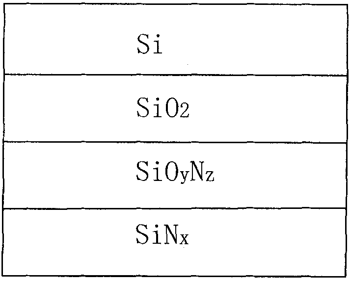
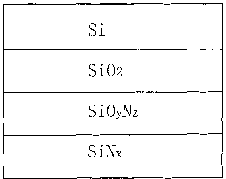
[0015] The method for realizing the slowly-varying laminated passivation film on the back surface of the solar cell is to deposit the film on the backlight surface of the silicon wafer of the solar cell after treatment by a chemical vapor deposition process, and the gas at the beginning of the deposition process is SiH 4 and N 2 A mixed gas of O, gradually adding NH during the deposition process 3 , so that the composition of the film changes from silicon dioxide on the surface of the silicon wafer to silicon oxynitride on the outer layer and then to silicon nitride on the outer layer.

[0016] The chemical vapor deposition process is to deposit on the back of the silicon wafer at a temperature of 200°-400°. The silicon wafer is P-type or N-type single crystal silicon, and the resistivity of the silicon wafer is 0.2Ωcm-10Ωcm. The gas at the beginning of the chemical vapor deposition process is SiH 4 an...


PUM

PropertyMeasurementUnit
thicknessaaaaaaaaaa
thicknessaaaaaaaaaa

Abstract

The invention relates to the field of solar cell production method, especially to a method for realizing a laminated passivation film on the back surface of a solar cell. A film is deposited on the backlight surface of a processed solar cell silicon chip according to chemical vapor deposition technology, the mixed gas of SiH4 and N2O is adopted as the gas at the beginning of the deposition, NH3 is gradually added in the process of deposition so that the component of the film is changed from silicon dioxide on the surface of the silicon chip to nitrogen oxide of silicon in the outward direction and then to silicon nitride in the outward direction, and the thickness of the film ranges from 50nm to 300nm. The method has the characteristics of fast deposition speed, high output, being capable of achieving the deposition of a plurality of films at a time, and high tightness of the deposited film. High temperature process is not needed in the technology, the heat budget required is less, and high temperature influence resulted from thermal oxidization is avoided, in addition, such a graded laminated film can effectively reduce interface state caused by the combination of different films, improve thermal stability compared with silicon nitride only, and lessen film stress.

Description

technical field [0001] The invention relates to the field of solar cell production methods, in particular to a method for realizing a slowly-varying lamination passivation film on the back surface of the solar cell. Background technique [0002] Photovoltaic power generation is a very important field in the utilization of solar energy. It is an urgent task to seek new technologies, new materials, and new processes to improve battery conversion efficiency and reduce costs. [0003] The conversion efficiency of solar cells is directly related to the generated photovoltaic electron-hole pairs. More electron-hole pairs mean high conversion efficiency, but only when these minority electrons are actually collected can they be converted into electrical energy. Various defects and interface states of the silicon wafer will greatly recombine these minority carriers, reducing the final effective conversion efficiency. By improving the pulling technology of crystalline silicon, the de...

Claims


Application Information

Patent Timeline
Patent Type & Authority Applications(China)
IPC IPC(8): C23C16/52H01L31/18
CPCH01L31/02167Y02E10/50
Inventor 刘亚锋
Owner TRINA SOLAR CO LTD
Learn More