Photovoltaic organic infrared semiconductor detector

A detector and semiconductor technology, applied in semiconductor devices, semiconductor/solid-state device manufacturing, photovoltaic power generation, etc., can solve the problems such as the inability to meet the detection requirements of flexible substrates, the high cost of inorganic infrared photovoltaic detectors, and the need for cooling, and achieve power consumption. Low, easy-to-array, fast-response effects

Inactive Publication Date: 2011-02-23
KUNMING INST OF PHYSICS
View PDF4 Cites 1 Cited by
  • Summary
  • Abstract
  • Description
  • Claims
  • Application Information

AI Technical Summary

Problems solved by technology

[0005] The present invention aims to solve the problems that the inorganic infrared photovoltaic detector is costly, toxic, requires refrigeration, and cannot meet the detection requirements of a flexible substrate. It provides a photovoltaic type organic infrared semiconductor detector, which has the advantages of low cost, easy realization of large area, Large array, controllable resistivity of photosensitive materials, no need for refrigeration, flexible processing, etc., has important application value in military, civilian and some specific fields

Method used


Image

  • Photovoltaic organic infrared semiconductor detector
  • Photovoltaic organic infrared semiconductor detector
  • Photovoltaic organic infrared semiconductor detector

Examples


Embodiment 1

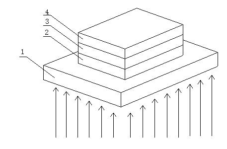
[0032] Embodiment 1: A bottom-detecting photovoltaic type organic infrared semiconductor detector, using a quartz plate as the substrate 1, depositing 150nm AZO on the substrate 1 by thermal evaporation to form a high work function electrode layer 2, and dissolving it with DMSO Erbium phthalocyanine, and then spin-coat 100nm erbium phthalocyanine on the high work function electrode layer 2 with a homogenizer to form an organic infrared semiconductor layer 3, and finally deposit 150nm Mg:Ag alloy by thermal evaporation technology to form a low work function electrode layer 4.

Embodiment 2

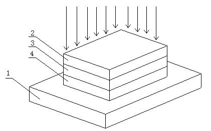
[0033]Embodiment 2: a kind of top detection photovoltaic type organic infrared semiconductor detector, with quartz sheet as substrate 1, the Nb of 150nm is deposited on substrate 1 with magnetron sputtering method to form low work function electrode layer 4, then heat 100nm erbium phthalocyanine was deposited by evaporation technology to form organic infrared semiconductor layer 3 , and finally 150nm ITO was deposited by magnetron sputtering to form high work function electrode layer 2 .

Embodiment 3

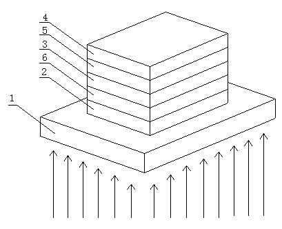
[0034] Embodiment 3: a kind of bottom detection photovoltaic type organic infrared semiconductor detector, with quartz sheet as substrate 1, deposit the ITO of 200nm on substrate 1 with the method for magnetron sputtering, form high work function electrode layer 2, then Deposit 10nm TPD sequentially by thermal evaporation technology to form hole transport layer 6, 150nm gadolinium phthalocyanine to form organic infrared semiconductor layer 3, 10nm Alq 3 An electron transport layer 5 is formed, and finally a 150nm Mg:Ag alloy is deposited by thermal evaporation to form a low work function electrode layer 4 .


PUM


Abstract

The invention relates to the technical field of photoelectricity, in particular to a photovoltaic organic infrared semiconductor detector. In the photovoltaic organic infrared semiconductor detector, a substrate made of special material is provided with functional layers made of special materials to form a three-layered, five-layered or seven-layered structure. The photovoltaic organic infrared semiconductor detector of the invention can be prepared on a Si-based substrate, an amorphous glass, a quartz substrate, a polycrystalline ceramic substrate and a flexible plastic substrate, is easy to realize a large-area array, and has the advantages of low cost, no need of refrigeration, flexibility and the like. The electrical parameter of a photosensing material is controllable, so that the resistance of devices can be regulated and controlled within the range of three orders of magnitude by doping, and the regulation of the device performance and the compatibility with an infrared system are improved.

Description

technical field [0001] The invention relates to the field of optoelectronic technology, in particular to a photovoltaic type organic infrared semiconductor detector. Background technique [0002] Infrared light is an electromagnetic wave that cannot be directly observed by the human eye and has a wavelength greater than 760nm, which is between visible light and microwaves. To convert this infrared light into a detectable physical quantity, the usual practice is to convert it into a quantitative electrical signal. An infrared detector is a device that converts an invisible incident infrared radiation signal into a detectable electrical signal output. [0003] Infrared detectors are divided into photoconductive detectors and photovoltaic detectors according to their working principles. Among them, photovoltaic detectors are devices made by utilizing the photovoltaic effect. Compared with photoconductive detectors, photovoltaic detectors have the advantages of fast response,...

Claims


Application Information

Patent Timeline
Patent Type & Authority Applications(China)
IPC IPC(8): H01L51/46H01L51/42H01L51/44
CPCY02E10/50Y02E10/549
Inventor 姬荣斌唐利斌宋立媛陈雪梅马钰王忆锋
Owner KUNMING INST OF PHYSICS
Why Eureka
Try Eureka