

Antireflection material for solar cell and manufacturing method thereof
A solar cell and anti-reflection technology, applied in circuits, electrical components, semiconductor devices, etc., to achieve the effects of promoting the solar industry, excellent optical properties, and good thermal stability
- Summary
- Abstract
- Description
- Claims
- Application Information
AI Technical Summary
Problems solved by technology
Method used
Image

Examples
Embodiment 1
[0040] A kind of anti-reflection material for solar cells, namely Al 2 o 3 The ErAlO amorphous composite oxide film with a mole percentage of 30%.
[0041] Er 2 o 3 / Al 2 o 3 A 7:3 mixed ceramic target is formed by sputtering on a P-type Si(100) substrate; the resistivity of the selected silicon wafer is 2-10 Ω·cm, the substrate temperature is room temperature, and surface treatment is required before growth. The RF power is 40 W, and the sputtering gas is Ar and O 2 , oxygen partial pressure ratio P=P(O 2 ) / ((P(O 2 )+P(Ar)) is 1%, and the working pressure is 1.0 Pa. P-type (100) silicon wafers with a resistivity of 2-10 Ω cm were ultrasonically cleaned with deionized water for 10 min before growth, and then etched with 1% HF acid for 30 s to remove the natural oxide layer on the surface of the Si substrate. , and finally sent to the growth chamber. The thickness of the obtained ErAlO thin film was 90 nm, and the annealing treatment was carried out in an annealing fu...
Embodiment 2
[0043] A kind of anti-reflection material for solar cells, namely Al 2 o 3 The ErAlO amorphous oxide film with a mole percentage of 0%.
[0044] Er 2 o 3 The ceramic target is formed by sputtering on a P-type Si(100) substrate; the resistivity of the selected silicon wafer is 2-10 Ω·cm, the temperature of the substrate is room temperature, and surface treatment is required before growth. The RF power is 40 W, and the sputtering gas is Ar and O 2 , oxygen partial pressure ratio P=P(O 2 ) / ((P(O 2 )+P(Ar)) is 1%, and the working pressure is 1.0 Pa. P-type (100) silicon wafers with a resistivity of 2-10 Ω cm were ultrasonically cleaned with deionized water for 10 min before growth, and then etched with 1% HF acid for 30 s to remove the natural oxide layer on the surface of the Si substrate. , and finally sent to the growth chamber. The thickness of the obtained ErAlO thin film was 90 nm, and the annealing treatment was carried out in an annealing furnace with an oxygen flo...
Embodiment 3
[0046] Changed Al in ErAlO film 2 o 3 content, with Al 2 o 3 Al with a molar content of 20% 2 o 3 -Er 2 o 3 A mixed ceramic target is used as a sputtering target, and other manufacturing conditions are the same as in Example 1.
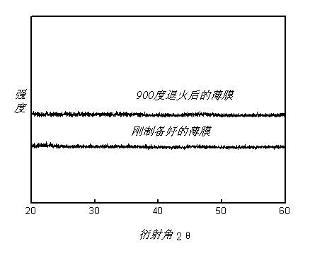
[0047] figure 1 It is the XRD spectrum before and after 900 ℃ of annealing of the thin film of embodiment 1, from figure 1 It can be seen that the film of Example 1 does not have any characteristic diffraction peaks, indicating that when the substrate temperature is room temperature, the ErAlO film deposited on the Si(100) substrate by radio frequency sputtering is in an amorphous state. No obvious crystallization occurred in the film during annealing at 900℃.
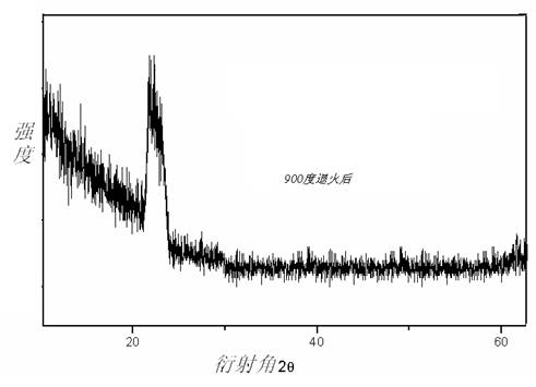
[0048] figure 2 It is the XRD spectrum of Example 2, whether it is under nitrogen atmosphere or under oxygen atmosphere, after annealing at 900 ℃, Er 2 o 3 The XRD analysis of the thin film shows that there are silicate diffraction peaks, and the samples are unstable when annealed...
PUM
| Property | Measurement | Unit |
|---|---|---|
| Resistivity | aaaaa | aaaaa |
| Thickness | aaaaa | aaaaa |
| Refractive index | aaaaa | aaaaa |
Abstract
Description
Claims
Application Information