
Method for packaging LED (light emitting diode)

A technology of LED packaging and LED chips, which is applied in the direction of semiconductor devices, electrical components, circuits, etc., can solve the problems that the improvement of LED light output efficiency is not very obvious or lower, and achieve the effect of improving light output efficiency and uniform aperture size

Active Publication Date: 2011-04-06
SINO INNOV SEMICON (PKU) CO LTD
View PDF5 Cites 12 Cited by
  • Summary
  • Abstract
  • Description
  • Claims
  • Application Information

AI Technical Summary

Problems solved by technology

Although these methods can effectively improve and increase the light extraction efficiency of bare chip LEDs, after the die is packaged, due to the surrounding of epoxy resin, the higher light extraction efficiency obtained by using the above methods will be partially eliminated and reduced. In the end, the improvement of the light output efficiency of the packaged LED is not very obvious

Method used

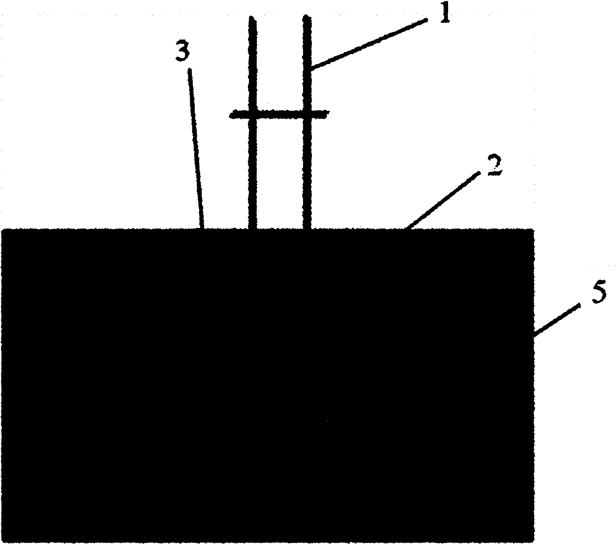

Image

  • Method for packaging LED (light emitting diode)
  • Method for packaging LED (light emitting diode)
  • Method for packaging LED (light emitting diode)

Examples


Embodiment 1

[0020] Example 1: In-line packaging of small die GaN-based blue LED with AAO film attached to the inner surface of the mold

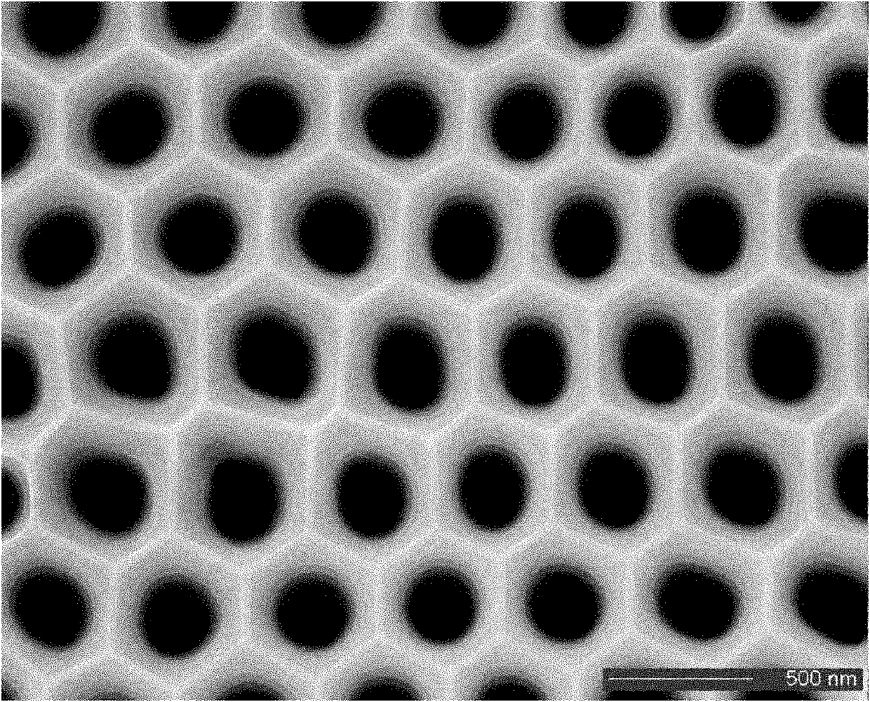
[0021] 1. Put the electropolished aluminum foil into a phosphoric acid solution, and prepare a periodic microstructure AAO film with a hole spacing close to 460nm (the emission wavelength of the blue LED tube core) by secondary anodic oxidation. Remove the aluminum substrate with a saturated copper chloride solution, and then expand the pores with a 5% phosphoric acid solution to obtain a periodic microstructured AAO template with a pore diameter of about 270 nm, such as figure 1 .

[0022] 2. Spread the AAO film with periodic microstructure prepared in step 1 evenly on the inner surface of the packaging mold.

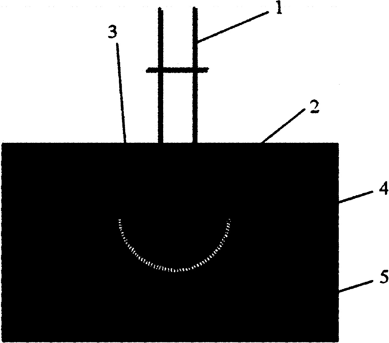
[0023] 3. Inject liquid epoxy resin into the mold, and then insert the pressure-welded LED bracket into the silicon mold. The small die GaN-based blue LED has a light emission wavelength of about 460nm, such as figure 2 shown. Then it is bak...

Embodiment 2

[0024] Example 2: Encapsulating a small die GaN-based blue LED with a silicon mold prepared by an AAO template

[0025] 1. Put the electropolished aluminum foil into phosphoric acid solution, and prepare a periodic microstructure AAO film with a pore spacing of about 460 nm by secondary anodic oxidation. Remove the aluminum substrate with a saturated copper chloride solution, and then expand the pores with a 5% phosphoric acid solution to obtain a periodic microstructured AAO template with a pore diameter of about 270 nm, such as figure 1 .

[0026] 2. Spread the AAO film with periodic microstructure prepared in step 1 evenly on the inner surface of the silicon mold.

[0027] 3. Use the AAO template as a mask, etch the silicon mold with dry etching technology, and then remove the AAO template to obtain a reusable silicon packaging mold with a periodic microstructure on the inner surface.

[0028] 4. Spray the release agent on the inner surface of the silicon mold, then injec...

Embodiment 3

[0029] Embodiment 3: High-power vertical structure GaN-based blue LED chip packaging

[0030] 1. Put the electropolished aluminum foil into phosphoric acid solution, and prepare a periodic microstructure AAO film with a pore spacing of about 460 nm by secondary anodic oxidation. Remove the aluminum substrate with a saturated copper chloride solution, and then expand the pores with a 5% phosphoric acid solution to obtain a periodic microstructure through-hole AAO template with a pore diameter of about 270 nm, such as figure 1 .

[0031] 2. Spread the AAO film with a periodic microstructure prepared in step 1 evenly on the surface of the high-power vertical structure LED die n-GaN, and then use inductively coupled plasma (ICP) etching, the etching of n-GaN The depth is about 1um. After the etching is completed, the AAO template on the surface of the die is removed to obtain an n-GaN light-emitting surface with a periodic microstructure.

[0032] 3. Fix the high-power vertical...


PUM

PropertyMeasurementUnit
Diameteraaaaaaaaaa
Apertureaaaaaaaaaa

Abstract

The invention provides a method for packaging an LED (Light Emitting Diode), which belongs to the technical field of photoelectric devices. In the invention, an AAO (Anode Alumina Oxidation) template is used for preparing a periodic microstructure on epoxy resin in the process of packaging. The method comprises the following specific steps of: firstly, preparing the AAO template of the periodic microstructure matched with the wavelength of an LED chip to be packaged; secondly, uniformly spreading the AAO template on the inner surface of an LED packaging mould; lastly, casting the liquid epoxy resin in the mould; carrying out vacuum degassing; putting the mould in an oven for baking; and taking down the packaged device from the mould after the epoxy resin is solidified, wherein the outer surface of the epoxy resin of the LED device has the same periodic microstructure as the AAO mould. In the invention, the packaging mould which can be reused and has the periodic microstructure is further prepared by using the AAO mould. In the invention, the optical performance of the device is improved by transferring the periodic microstructure on the AAO template to the epoxy resin which is an LED packing material, and therefore light-extraction efficiency is improved.

Description

technical field [0001] The invention belongs to the technical field of photoelectric devices, and in particular relates to an LED packaging method. Background technique [0002] Semiconductor light-emitting diodes (LEDs) have the characteristics of high brightness, low energy consumption, long life, and fast response. Although the internal quantum efficiency of LEDs can reach a relatively high level, the light extraction efficiency of LED devices is very low due to the high refractive index of the material, which eventually leads to low external quantum efficiency of LEDs. Therefore, improving the light extraction efficiency of LEDs has become a problem that needs to be solved urgently, and has aroused people's extensive attention and research. In recent years, the main methods for people to improve the light output efficiency of LEDs include: using PSS substrates when growing epitaxial wafers; adding bottom reflectors during chip manufacturing, corroding the sidewall of th...

Claims


Application Information

Patent Timeline
IPC IPC(8): H01L33/00H01L33/48
Inventor 于彤军邓俊静付星星康香宁陈志忠张国义
Owner SINO INNOV SEMICON (PKU) CO LTD
Learn More