

Preparation method of CuInS2 nanocrystalline material
A nanocrystalline material and nanocrystalline technology are applied in the growth of polycrystalline materials, chemical instruments and methods, and single crystal growth. It can solve the problems of unsuitable large-scale preparation, poor dispersion of nanoparticles, and high cost. It is suitable for large-scale Large-scale industrial production, mild reaction conditions, and the effect of reducing production costs
- Summary
- Abstract
- Description
- Claims
- Application Information
AI Technical Summary
Problems solved by technology
Method used
Image

Examples
Embodiment 1
[0032] CuInS 2 The preparation method of nanocrystalline materials, taking the preparation of S1 sample as an example, the steps are as follows:
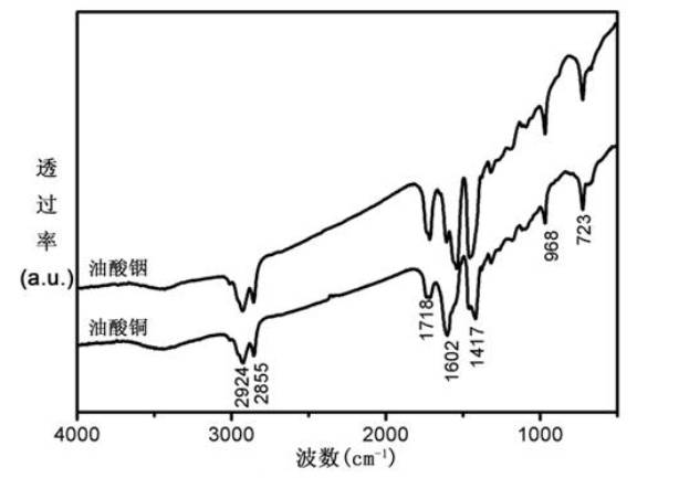
[0033]1) Dissolve 20 mmol sodium oleate and 10 mmol copper chloride or 10 mmol indium chloride in a mixed solution of 30 mL n-hexane, 15 mL deionized water and 20 mL ethanol and reduce Pressure distillation, then stirred at 60 oC for 4h, then washed 5 times with water and rotary evaporated to remove the remaining n-hexane, to obtain the precursor copper oleate and indium oleate;
[0034] 2) Mix 1mmol of the prepared precursor copper oleate and indium oleate mixture with 2ml oleic acid (OA), put 15ml oleylamine solvent dissolved in 1mmol elemental sulfur into the above mixed solution, at a temperature of 80°C, Under the vacuum condition of -0.1MPa, react for 30 minutes, fill with Ar, and finally react for 60 minutes under stirring at 180°C to form a black-red product;
[0035] 3) After the obtained product was cooled to room temper...
Embodiment 2
[0042] CuInS 2 The preparation method of nanocrystalline material, taking the preparation of S4 sample as an example, the steps are as follows:
[0043] 1) Dissolve 20 mmol sodium oleate and 10 mmol copper chloride or 10 mmol indium chloride in a mixed solution of 30 mL n-hexane, 15 mL deionized water and 20 mL ethanol and reduce Pressure distillation, then stirred at 60 oC for 4h, then washed 5 times with water and rotary evaporated to remove the remaining n-hexane, to obtain the precursor copper oleate and indium oleate;
[0044] 2) Mix 1mmol of the prepared precursor copper oleate and indium oleate mixture with 2ml of oleic acid (OA), put 6ml of oleylamine solvent dissolved in 1mmol of elemental sulfur into the above mixed solution, at a temperature of 90°C, Under the vacuum condition of -0.05MPa, react for 45 minutes, fill with Ar, and finally react for 45 minutes under stirring at 180°C to form a black-red product;
[0045] 3) After the obtained product was cooled to ro...
Embodiment 3
[0051] CuInS 2 The preparation method of nanocrystalline materials, taking the scale-up preparation of S1 samples as an example:
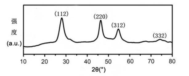
[0052] According to Example 1, the amount of the reactant copper oleate, indium oleate precursor and elemental sulfur was increased to 20 times the original amount, that is, the precursor copper oleate and indium oleate mixture was 20mmol, and the oleic acid was 40ml , elemental sulfur is 20mmol, oleylamine is 300ml, CuInS with a particle size of about 9.7nm can be obtained under the same conditions 2 Nanocrystalline pure phases, such as Figure 8 shown. This shows that the CuInS provided by the present invention 2 The preparation method of the nanocrystalline material can be used for large-scale industrial production.
[0053] The results show that the CuInS provided by the invention 2 The preparation method of the nanocrystalline material has controllable product size, good dispersion, simple operation, easy repeatability, high purity, mild ...
PUM
 Abstract
Description
Claims
Application Information