Beta irradiation detector based on silicon carbide junction field-effect transistor (JFET)

A technology of irradiation detectors and silicon carbide junctions, which is applied in the directions of radiation intensity measurement, semiconductor devices, sustainable manufacturing/processing, etc., can solve the problems of weakening device detection capabilities, reducing channel currents, etc., and eliminate surface trap effects , Improving device performance and strong radiation resistance

Active Publication Date: 2011-05-25
陕西半导体先导技术中心有限公司
View PDF4 Cites 13 Cited by
  • Summary
  • Abstract
  • Description
  • Claims
  • Application Information

AI Technical Summary

Problems solved by technology

However, since this structure does not involve the buffer layer, under the irradiation of nuclear rays, the incident rays will cause the surface trap effect, absorb the number of carriers in the channel, reduce the channel current, and weaken the detection capability of the device, so it is not suitable Make a Radiation Detector

Method used


Image

  • Beta irradiation detector based on silicon carbide junction field-effect transistor (JFET)
  • Beta irradiation detector based on silicon carbide junction field-effect transistor (JFET)
  • Beta irradiation detector based on silicon carbide junction field-effect transistor (JFET)

Examples


Embodiment 1

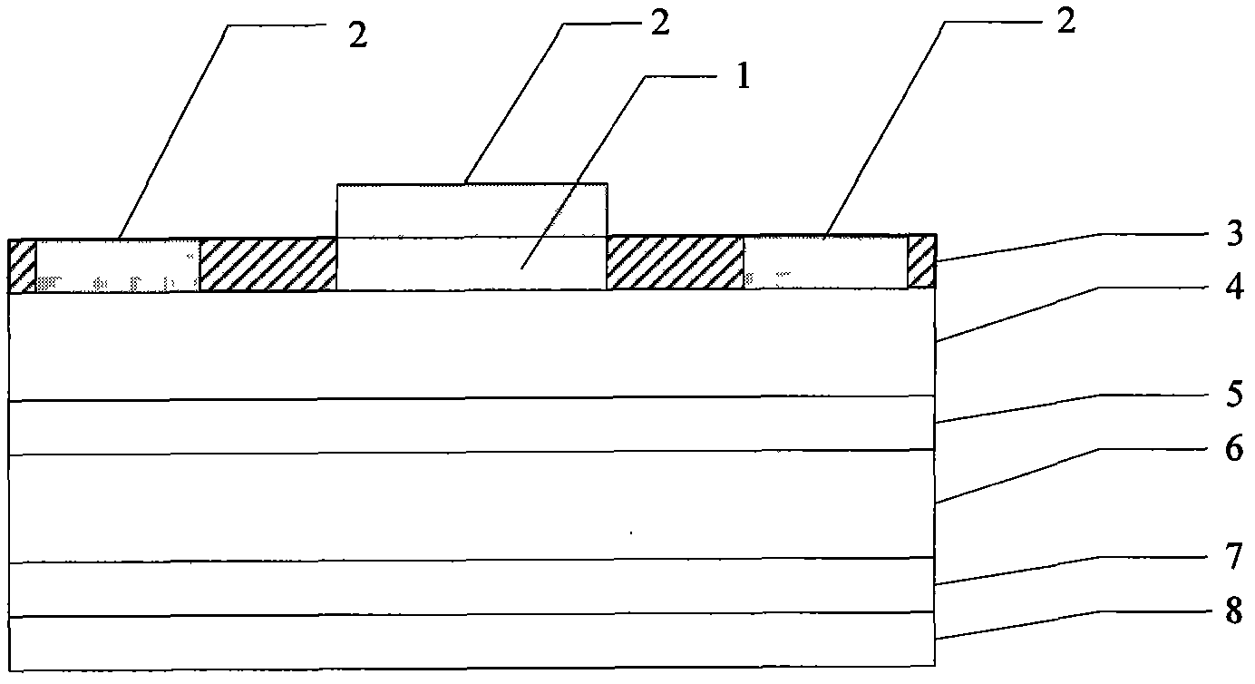
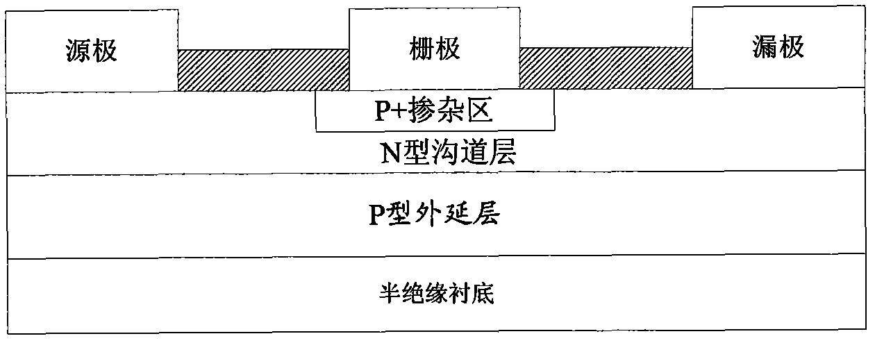
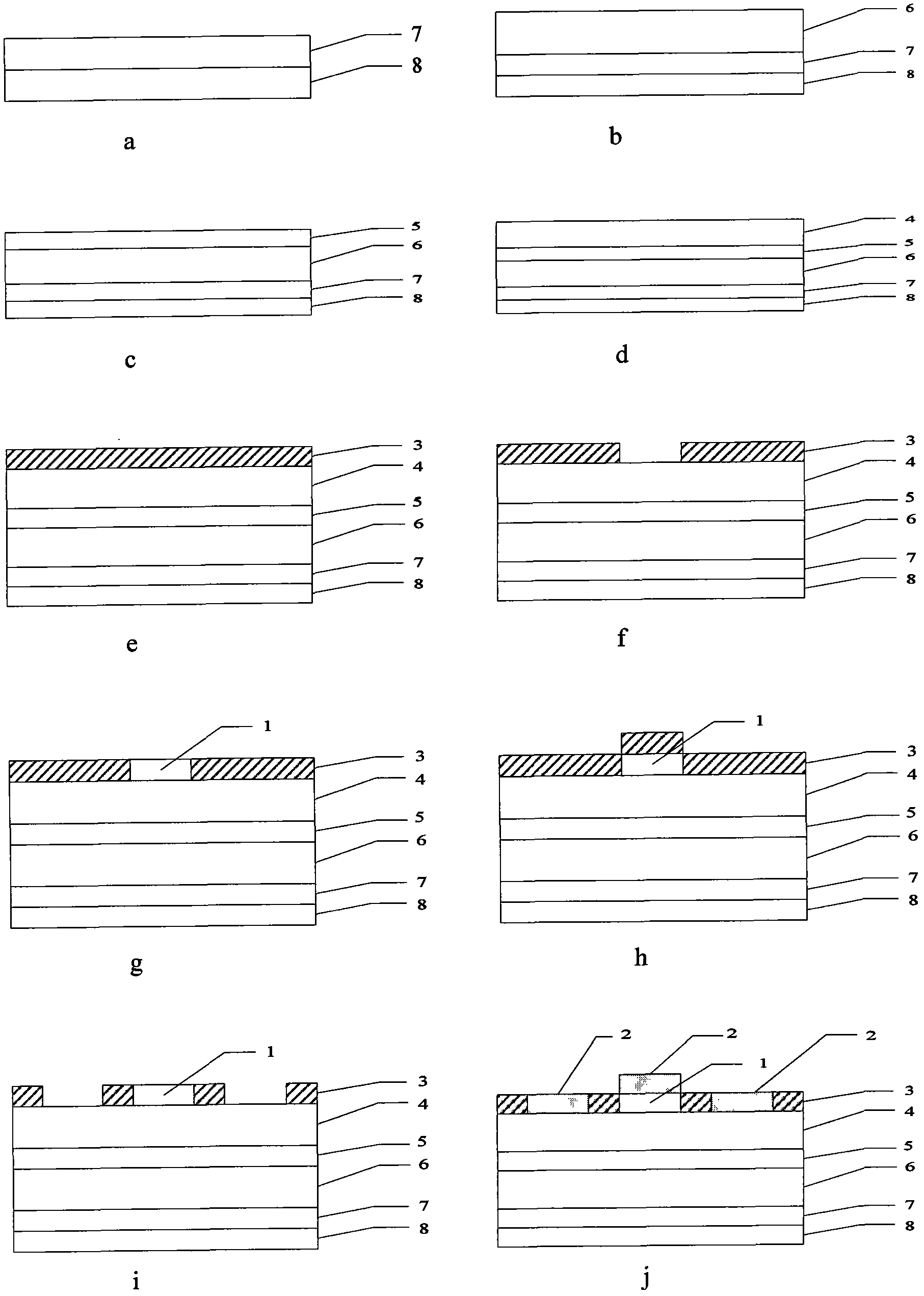
[0032] Step 1. Use a doping concentration of 5×10 17 cm -3 , an N-type 4H-SiC substrate with a thickness of 0.4 μm is used as the substrate 8, and the epitaxial growth doping concentration is 1.0×10 15 cm -3 , a P-type buffer layer 7 with a thickness of 0.1 μm, such as image 3 a, The epitaxy process conditions are: temperature is 1570°C, pressure is 100Mbar, growth gas is C 3 h 8 、SiH 4 and H 2 , where H 2 To carry gas.

[0033] Step 2. Epitaxial N-type channel 6 on the P-type buffer layer with a doping concentration of 1×10 16 cm -3 , with a thickness of 0.4 μm, such as image 3 b. The process conditions of the epitaxy are: temperature is 1570°C, pressure is 100Mbar, growth gas is C 3 h 8 、SiH 4 and H 2 , where H 2 To carry gas.

[0034] Step 3. The epitaxial doping concentration on the upper part of the N-type channel 6 is 1.0×10 15 cm -3 , an N-type buffer layer 5 with a thickness of 0.1 μm, such as image 3 c. The process conditions of the epitaxy are: ...

Embodiment 2

[0042] The first step uses a doping concentration of 5×10 17 cm -3 , an N-type 4H-SiC substrate with a thickness of 0.4 μm is used as the substrate 8, and the epitaxial growth doping concentration is 2.5×10 15 cm -3 , a P-type buffer layer 7 with a thickness of 0.15 μm, the epitaxy process conditions are temperature 1570°C, pressure 100Mbar, growth gas C 3 h 8 、SiH 4 and H 2 , where H 2 To carry gas, such as image 3 a;

[0043] In the second step, the epitaxial doping concentration on the P-type buffer layer is 1×10 16 cm -3 , an N-type channel 6 with a thickness of 0.4 μm, such as image 3 b. The process conditions of the epitaxy are: temperature is 1570°C, pressure is 100Mbar, growth gas is C 3 h 8 、SiH 4 and H 2 , where H 2 To carry gas.

[0044] In the third step, the epitaxial doping concentration on the upper part of the N-type channel 6 is 2.5×10 15 cm -3 , an N-type buffer layer 5 with a thickness of 0.15 μm, such as image 3 c. The process conditio...

Embodiment 3

[0052] Step A uses a doping concentration of 5×10 17 cm -3 , an N-type 4H-SiC substrate with a thickness of 0.4 μm is used as the substrate 8, and the epitaxial growth doping concentration is 5.0×10 15 cm -3 , a P-type buffer layer 7 with a thickness of 0.2 μm, the epitaxy process conditions are temperature 1570°C, pressure 100Mbar, growth gas C 3 h 8 、SiH 4 and H 2 , where H 2 To carry gas, such as image 3 a.

[0053] Step B epitaxial N-type channel 6 on the P-type buffer layer, the doping concentration is 1×10 16 cm -3 , with a thickness of 0.4 μm, such as image 3 b. The process conditions of the epitaxy are: temperature is 1570°C, pressure is 100Mbar, growth gas is C 3 h 8 、SiH 4 and H 2 , where H2 To carry gas.

[0054] In step C, the epitaxial doping concentration on the upper part of the N-type channel 6 is 5.0×10 15 cm -3 , an N-type buffer layer 5 with a thickness of 0.2 μm, such as image 3 c. The process conditions of the epitaxy are: temperature ...


PUM


Abstract

The invention discloses a beta ray irradiation detector based on a silicon carbide metal-semiconductor field effect transistor structure, which is used for mainly solving the problems of poor irradiation resistance and low energy conversion efficiency of an existing beta irradiation detector. The detector comprises an n-type substrate (8), a p-type buffer layer (7), an n-type channel (6) with the concentration of 3.5*10<17>cm<-3> to 4*10<17>cm<-3>, an n-type buffer layer (5) and an ohmic contact layer (4) from top to bottom, wherein a source and a drain (2) are deposited on the ohmic contact layer; a semitransparent Schottky contact layer (1) is deposited on the n-type buffer layer; the Schottky contact layer is formed by high barrier Schottky metals of Au, Ti and Pt, and is embedded in the n-type buffer layer (5) with the depth of 0.06-0.08 mu m; and a surface area except a grid electrode as well as the source and drain is covered with a SiO2 passivation layer (3). The beta ray irradiation detector has the characteristics of strong resistance to radiation, high energy conversion efficiency and high detection efficiency, and can be applied to detecting beta rays in nuclear energy.

Description

technical field [0001] The invention belongs to the field of microelectronics, and in particular relates to a beta ray radiation detector based on a silicon carbide junction field effect transistor structure, which can be used in the field of beta ray ionizing radiation detection in nuclear energy. technical background [0002] Semiconductor radiation detector is a new type of advanced detector developed after gas detector and scintillator detector. The basic principle is to use semiconductor technology, such as evaporation, diffusion, ion implantation, etc., to make a thicker depletion layer or diffusion region on the semiconductor substrate under the working condition of reverse bias voltage, which is used to detect incident rays or charged particles. Existing semiconductor radiation detectors are all based on Si, GaAs materials such as diodes and PIN tubes, and are mainly used to detect alpha particles, beta rays and neutrons. [0003] Semiconductor radiation detectors ...

Claims


Application Information

Patent Timeline
Patent Type & Authority Applications(China)
IPC IPC(8): H01L31/119H01L31/0352G01T1/24H01L31/18
CPCY02P70/50
Inventor 郭辉洪朴张玉明张义门程和远詹晓伟
Owner 陕西半导体先导技术中心有限公司
Why Eureka
Try Eureka