

Solution for nickel electroforming, electroforming method using solution and thin nickel plate manufactured by using method
An electroforming, solution technology, applied in electroforming, electrolytic processes, etc., can solve the problems of uneven opening size, curling or warping, insufficient thickness uniformity around micropore openings, etc., and achieve compressive stress and/or Low tensile stress, balanced compressive stress and tensile stress, simple effect of graphic transfer link
- Summary
- Abstract
- Description
- Claims
- Application Information
AI Technical Summary
Problems solved by technology
Method used
Image

Examples
preparation example Construction
[0057] The present invention has no special limitation on the preparation method of the nickel electroforming solution, for example, the concentrated nickel sulfamate solution of concentration such as 180g / L can be diluted with deionized water, and then other components are added according to the stated concentration Can be prepared.
[0058] The amount of the auxiliary brightener in the nickel electroforming solution can be calculated each time according to the product of the required current and time during electroforming. Preferably, the amount of the auxiliary brightener is 0.1g / L / (100A×h)~0.15g / L / (100A×h), for example, it can be 0.1g / L / (100A×h), 0.11g / L / (100A×h), 0.12g / L / (100A×h), 0.13g / L / (100A×h), 0.14g / L / (100A×h) or 0.15g / L / (100A× h)). For example, if a current of 80A is used for electroforming for 0.5 hours, the product of the required current and time is 40A×h, and the concentration of the auxiliary brightener in the nickel electroforming solution should be 0.04g / L...
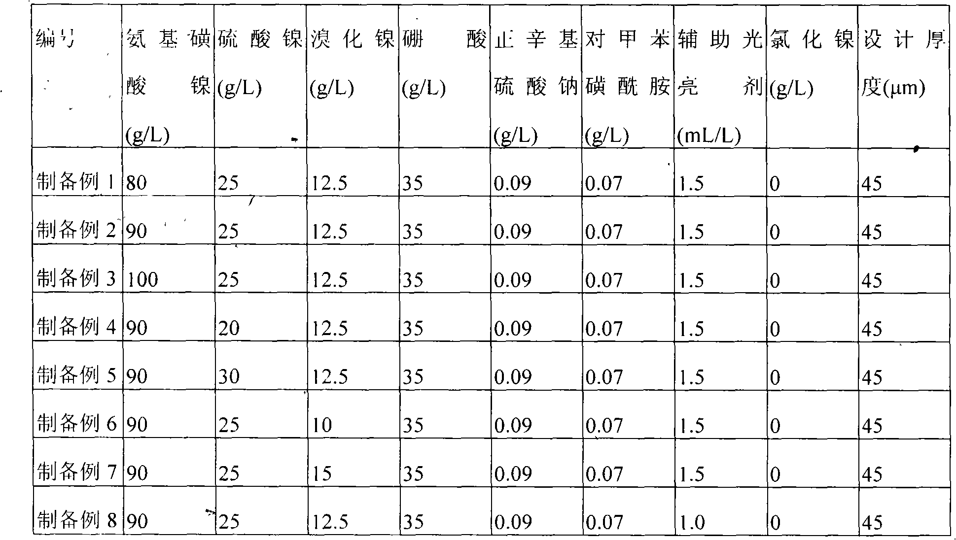
preparation example 1~8 and comparative example 1~3
[0085] A solution for nickel electroforming was prepared with deionized water according to the concentration in Table 1 below, wherein the auxiliary brightener was added in the form of a 100 g / L aqueous solution.
[0086] Table 1 is used for the concentration of each component of nickel electroforming solution
[0087]
[0088]
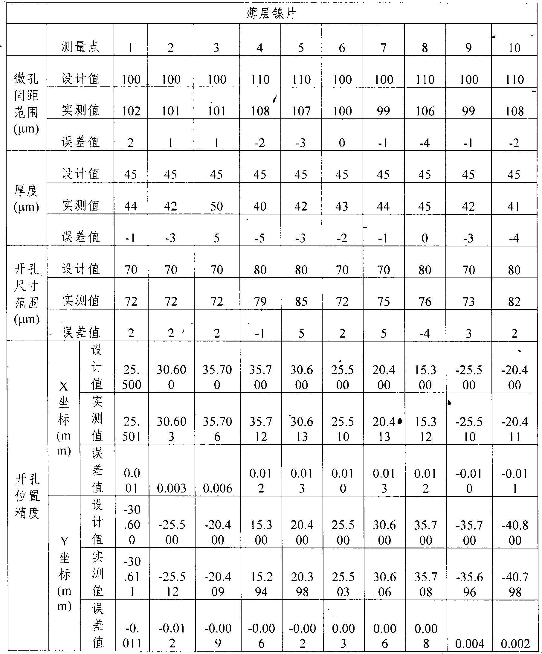
Embodiment 1
[0090] Thin-layer nickel sheets were prepared according to the following steps (see Table 3 for specific process parameters), wherein the electroforming solution for nickel electroforming prepared in Preparation Example 1 was used for electroforming, and a bidirectional pulse power supply was used as the electroforming power supply.
[0091] Activation: Put a bright stainless steel substrate (purchased from Changtai Stainless Steel Technology Group, 1.5mm thick 304 mirror stainless steel) in the activation tank (the solution is industrial hydrochloric acid and deionized water in a volume ratio of 1:4) Activated in medium for 30 minutes.
[0092] Lamination film: A layer of photosensitive film for electroforming (purchased from DuPont, thickness 50 μm, type HM1056) with a thickness of 50 μm is pressed on the surface of the stainless steel substrate.
[0093] Pattern transfer: make a high-precision chrome plate with the microhole pattern to be made in advance, and then use the c...
PUM
| Property | Measurement | Unit |
|---|---|---|
| Thickness | aaaaa | aaaaa |
Abstract
Description
Claims
Application Information